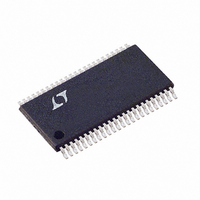
LTC1852IFW#PBF Linear Technology, LTC1852IFW#PBF Datasheet - Page 8

LTC1852IFW#PBF
Manufacturer Part Number
LTC1852IFW#PBF
Description
IC A/D CONV 8CH 10BIT 48-TSSOP
Manufacturer
Linear Technology
Datasheet
1.LTC1853CFWPBF.pdf
(24 pages)
Specifications of LTC1852IFW#PBF
Number Of Bits
10
Sampling Rate (per Second)
400k
Data Interface
Parallel
Number Of Converters
1
Power Dissipation (max)
15mW
Voltage Supply Source
Single Supply
Operating Temperature
-40°C ~ 85°C
Mounting Type
Surface Mount
Package / Case
48-TFSOP (0.240", 6.10mm Width)
Lead Free Status / RoHS Status
Lead free / RoHS Compliant
Available stocks
Company
Part Number
Manufacturer
Quantity
Price
LTC1852/LTC1853
PIN FUNCTIONS
D9/S0 (Pin 23, LTC1853): Three-State Digital Data Outputs.
Active when RD is low. Following a conversion, bit 9 of the
present conversion is available on this pin. In Readback
mode, the end of sequence bit of the current sequencer
location (S0) is available on this pin. The output swings
between OV
D6 to D0 (Pins 24 to 30, LTC1852): Three-State Digital
Data Outputs. Active when RD is low. The outputs swing
between OV
D8 to D0 (Pins 24 to 32, LTC1853): Three-State Digital
Data Outputs. Active when RD is low. The outputs swing
between OV
NC (Pins 31 to 32, LTC1852): No Connect. There is no
internal connection to these pins.
BUSY (Pin 33): Converter Busy Output. The BUSY output
has two functions. At the start of a conversion, BUSY will
go low and remain low until the conversion is completed.
The rising edge may be used to latch the output data.
BUSY will also go low while the part is in Program/Read-
back mode (M1 high, M0 low) and remain low until M0
is brought back high. The output swings between OV
and OGND.
OGND (Pin 34): Digital Data Output Ground. Tie to analog
ground plane. May be tied to logic ground if desired.
OV
to 5V, can be used to interface with 3V digital logic. Bypass
to OGND with 10μF tantalum in parallel with 0.1μF ceramic
or 10μF ceramic.
M0 (Pin 36): Mode Select Pin 0. Used in conjunction with
M1 to select operating mode. See Table 5.
PGA (Pin 37): Gain Select Input. A high logic level selects
gain = 1, a low logic level selects gain = 2.
8
DD
(Pin 35): Digital Data Output Supply. Normally tied
DD
DD
DD
and OGND.
and OGND.
and OGND.
DD
UNI/BIP (Pin 38): Unipolar/Bipolar Select Input. Logic low
selects a unipolar input span, a high logic level selects a
bipolar input span.
A0 to A2 (Pins 39 to 41): MUX Address Input Pins.
DIFF (Pin 42): Single-Ended/Differential Select Input.
A low logic level selects single ended, a high logic level
selects differential.
WR (Pin 43): Write Input. In Direct Address mode, WR
low enables the MUX address and confi guration input pins
(Pins 37 to 42). WR can be tied low or the rising edge of
WR can be used to latch the data. In Program mode, WR
is used to program the sequencer. WR low enables the
MUX address and confi guration input pins (Pins 37 to 42).
The rising edge of WR latches the data and increments
the counter to the next sequencer location.
RD (Pin 44): Read Input. During normal operation, RD
enables the output drivers when CS is low. In Readback
mode (M1 high, M0 low), RD going low reads the cur-
rent sequencer location, RD high advances to the next
sequencer location.
CONVST (Pin 45): Conversion Start Input. This active low
signal starts a conversion on its falling edge.
CS (Pin 46): Chip Select Input. The chip select input must
be low for the ADC to recognize the CONVST and RD inputs.
If SHDN is low, a low logic level on CS selects Nap mode;
a high logic level on CS selects Sleep mode.
SHDN (Pin 47): Power Shutdown Input. A low logic level
will invoke the Shutdown mode selected by the CS pin.
CS low selects Nap mode, CS high selects Sleep mode.
Tie high if unused.
M1 (Pin 48): Mode Select Pin 1. Used in conjunction with
M0 to select operating mode. See Table 5.
18523fa


