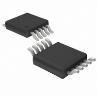
LTC2402CMS#PBF Linear Technology, LTC2402CMS#PBF Datasheet - Page 10

LTC2402CMS#PBF
Manufacturer Part Number
LTC2402CMS#PBF
Description
IC ADC 24BIT 2CH MICROPWR 10MSOP
Manufacturer
Linear Technology
Datasheet
1.LTC2401CMSPBF.pdf
(32 pages)
Specifications of LTC2402CMS#PBF
Number Of Bits
24
Sampling Rate (per Second)
7.5
Data Interface
MICROWIRE™, Serial, SPI™
Number Of Converters
2
Power Dissipation (max)
1mW
Voltage Supply Source
Single Supply
Operating Temperature
0°C ~ 70°C
Mounting Type
Surface Mount
Package / Case
10-TFSOP, 10-MSOP (0.118", 3.00mm Width)
Number Of Elements
1
Resolution
24Bit
Architecture
Delta-Sigma
Sample Rate
0.008KSPS
Input Polarity
Unipolar
Input Type
Voltage
Rated Input Volt
6.188V
Differential Input
Yes
Power Supply Requirement
Single
Single Supply Voltage (typ)
3.3/5V
Single Supply Voltage (min)
2.7V
Single Supply Voltage (max)
5.5V
Dual Supply Voltage (typ)
Not RequiredV
Dual Supply Voltage (min)
Not RequiredV
Dual Supply Voltage (max)
Not RequiredV
Integral Nonlinearity Error
15ppm of Vref
Operating Temp Range
0C to 70C
Operating Temperature Classification
Commercial
Mounting
Surface Mount
Pin Count
10
Package Type
MSOP
Lead Free Status / RoHS Status
Lead free / RoHS Compliant
Available stocks
Company
Part Number
Manufacturer
Quantity
Price
APPLICATIO S I FOR ATIO
LTC2401/LTC2402
Converter Operation Cycle
The LTC2401/LTC2402 are low power, delta-sigma ana-
log-to-digital converters with an easy to use 3-wire serial
interface. Their operation is simple and made up of three
states. The converter operating cycle begins with the
conversion, followed by a low power sleep state and
concluded with the data output (see Figure 1). The 3-wire
interface consists of serial data output (SDO), a serial
clock (SCK) and a chip select (CS).
Initially, the LTC2401/LTC2402 perform a conversion.
Once the conversion is complete, the device enters the
sleep state. While in this sleep state, power consumption
is reduced by an order of magnitude. The part remains in
the sleep state as long as CS is logic HIGH. The conversion
result is held indefinitely in a static shift register while the
converter is in the sleep state.
Once CS is pulled low, the device begins outputting the
conversion result. There is no latency in the conversion
result. The data output corresponds to the conversion just
performed. This result is shifted out on the serial data out
pin (SDO) under the control of the serial clock (SCK). Data
is updated on the falling edge of SCK allowing the user to
reliably latch data on the rising edge of SCK, see Figure 3.
The data output state is concluded once 32 bits are read
out of the ADC or when CS is brought HIGH. The device
automatically initiates a new conversion cycle and the
cycle repeats.
10
Figure 1. LTC2401/LTC2402 State Transition Diagram
U
1
DATA OUTPUT
CONVERT
U
CS AND
SCK
SLEEP
0
24012 F01
W
U
Through timing control of the CS and SCK pins, the
LTC2401/LTC2402 offer several flexible modes of opera-
tion (internal or external SCK and free-running conversion
modes). These various modes do not require program-
ming configuration registers; moreover, they do not dis-
turb the cyclic operation described above. These modes of
operation are described in detail in the Serial Interface
Timing Modes section.
Conversion Clock
A major advantage delta-sigma converters offer over
conventional type converters is an on-chip digital filter
(commonly known as Sinc or Comb filter). For high
resolution, low frequency applications, this filter is typi-
cally designed to reject line frequencies of 50Hz or 60Hz
plus their harmonics. In order to reject these frequencies
in excess of 110dB, a highly accurate conversion clock is
required. The LTC2401/LTC2402 incorporate an on-chip
highly accurate oscillator. This eliminates the need for
external frequency setting components such as crystals or
oscillators. Clocked by the on-chip oscillator, the LTC2401/
LTC2402 reject line frequencies (50Hz or 60Hz 2%) a
minimum of 110dB.
Ease of Use
The LTC2401/LTC2402 data output has no latency, filter
settling or redundant data associated with the conversion
cycle. There is a one-to-one correspondence between the
conversion and the output data. Therefore, multiplexing
an analog input voltage is easy.
The LTC2401/LTC2402 perform offset and full-scale cali-
brations every conversion cycle. This calibration is trans-
parent to the user and has no effect on the cyclic operation
described above. The advantage of continuous calibration
is extreme stability of offset and full-scale readings with
respect to time, supply voltage change and temperature
drift.
Power-Up Sequence
The LTC2401/LTC2402 automatically enter an internal
reset state when the power supply voltage V
below approximately 2.2V. This feature guarantees the
CC
drops


