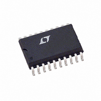
LTC1609CSW#TRPBF Linear Technology, LTC1609CSW#TRPBF Datasheet - Page 9

LTC1609CSW#TRPBF
Manufacturer Part Number
LTC1609CSW#TRPBF
Description
IC ADC SRL 16BIT 200KSPS 20-SOIC
Manufacturer
Linear Technology
Datasheet
1.LTC1609CSW.pdf
(24 pages)
Specifications of LTC1609CSW#TRPBF
Number Of Bits
16
Sampling Rate (per Second)
200k
Data Interface
Serial
Number Of Converters
1
Power Dissipation (max)
100mW
Voltage Supply Source
Analog and Digital
Operating Temperature
0°C ~ 70°C
Mounting Type
Surface Mount
Package / Case
20-SOIC (0.300", 7.50mm Width)
Lead Free Status / RoHS Status
Lead free / RoHS Compliant
Available stocks
Company
Part Number
Manufacturer
Quantity
Price
APPLICATIO S I FOR ATIO
the end of a conversion, the DAC output balances the V
input charge. The SAR contents (a 16-bit data word) that
represents the V
register.
Driving the Analog Inputs
The LTC1609 analog input ranges, along with the nominal
input impedances, are shown in Tables 1a and 1b. The
inputs are overvoltage protected to 25V. The input im-
pedance can get as low as 10k , therefore, it should be
driven with a low impedance source. Wideband noise
coupling into the input can be minimized by placing a
1000pF capacitor at the input as shown in Figure 2. An
NPO-type capacitor gives the lowest distortion. Place the
capacitor as close to the device input pin as possible. If an
amplifier is to be used to drive the input, care should be
taken to select an amplifier with adequate accuracy, linear-
ity and noise for the application. The following list is a
summary of the op amps that are suitable for driving the
LTC1609. More detailed information is available in the
Linear Technology data books and LinearView
LT1007 - Low noise precision amplifier. 2.7mA supply
current 5V to 15V supplies. Gain bandwidth product
8MHz. DC applications.
LT1097 - Low cost, low power precision amplifier. 300 A
supply current. 5V to 15V supplies. Gain bandwidth
product 0.7MHz. DC applications.
LT1227 - 140MHz video current feedback amplifier. 10mA
supply current. 5V to 15V supplies. Low noise and low
distortion.
LT1360 - 37MHz voltage feedback amplifier. 3.8mA sup-
ply current. 5V to 15V supplies. Good AC/DC specs.
Figure 2. Analog Input Filtering
A
A
A
IN1
IN2
IN3
IN
are loaded into the 16-bit output shift
U
200
100
U
1000pF
1000pF
1000pF
R1
R2
R3
W
LTC1609
IN
IN
IN
1609 F02
TM
U
CD-ROM.
IN
LT1363 - 50MHz voltage feedback amplifier. 6.3mA sup-
ply current. Good AC/DC specs.
LT1364/LT1365 - Dual and quad 50MHz voltage feedback
amplifiers. 6.3mA supply current per amplifier. Good
AC/DC specs.
LT1468 - 90MHz, 22V/ s 16-bit accurate amplifier
LT1469 - Dual LT1468
Offset and Gain Adjustments
The LTC1609 is specified to operate with three unipolar
and three bipolar input ranges. Pins R1
are connected as shown in Tables 1a and 1b for the
different input ranges. The tables also list the nominal
input impedance for each range. Table 1c shows the
output codes for the ideal input voltages of each of the six
input ranges.
The LTC1609 offset and full-scale errors have been trimmed
at the factory with the external resistors shown in Figures
3a and 3b. This allows for external adjustment of offset and
full scale in applications where absolute accuracy is im-
portant. The offset and gain adjustment circuits for the six
input ranges are also shown in Figures 3a and 3b. To
adjust the offset for a bipolar input range, apply an input
voltage equal to – 0.5LSB where 1LSB = (+ FS – – FS)/
65536 and change the offset resistor so the output code is
changing between 1111 1111 1111 1111 and 0000 0000
0000 0000. The gain is trimmed by applying an input
voltage of + FS – 1.5LSB and adjusting the gain trim resis-
tor until the output code is changing between 0111 1111
1111 1110 and 0111 1111 1111 1111. In both cases the
data is in two’s complement format (SB/BTC = LOW)
To adjust the offset for a unipolar input range, apply an
input voltage equal to + 0.5LSB where 1LSB = + FS/65536.
Then adjust the offset trim resistor until the output code
changes between 0000 0000 0000 0000 and 0000 0000
0000 0001. To adjust the gain, apply an input voltage equal
to + FS – 1.5LSB and vary the gain trimming resistor until
the output code is changing between 1111 1111 1111 1110
and 1111 1111 1111 1111. In the unipolar case, the data
is in straight binary format (SB/BTC = HIGH). Figures 4a
and 4b show the transfer characteristics of the LTC1609.
LinearView is a trademark of Linear Technology Corporation.
IN
LTC1609
, R2
IN
and R3
1609fa
9
IN


