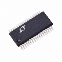
LTC1411CG#TRPBF Linear Technology, LTC1411CG#TRPBF Datasheet - Page 3

LTC1411CG#TRPBF
Manufacturer Part Number
LTC1411CG#TRPBF
Description
IC A/D CONV 14BIT 2.5MSPS 36SSOP
Manufacturer
Linear Technology
Datasheet
1.LTC1411IG.pdf
(16 pages)
Specifications of LTC1411CG#TRPBF
Number Of Bits
14
Sampling Rate (per Second)
2.5M
Data Interface
Parallel
Number Of Converters
1
Power Dissipation (max)
325mW
Voltage Supply Source
Analog and Digital
Operating Temperature
0°C ~ 70°C
Mounting Type
Surface Mount
Package / Case
36-SSOP (0.200", 5.30mm Width)
Lead Free Status / RoHS Status
Lead free / RoHS Compliant
DIGITAL I PUTS A D DIGITAL OUTPUTS
A ALOG I PUT
POWER REQUIRE E TS
SYMBOL PARAMETER
V
C
t
t
t
CMRR
I TER AL REFERE CE CHARACTERISTICS
PARAMETER
V
V
V
V
REFCOM2 Output Voltage
REFIN Input Current
The
SYMBOL PARAMETER
V
V
I
C
V
V
I
I
The
SYMBOL PARAMETER
V
I
P
ACQ
AP
jitter
IN
SOURCE
SINK
DD
U
IN
IN
REF
REF
REF
REF
IH
IL
IN
OH
OL
DD
D
U
Output Voltage
Output Tempco
Line Regulation
Load Regulation
denotes specifications which apply over the full operating temperature range, otherwise specifications are T
denotes specifications which apply over the full operating temperature range, otherwise specifications are T
Analog Input Range (Note 9)
Common Mode Input Range
Analog Input Capacitance
Sample-and-Hold Acquisition Time
Sample-and-Hold Aperture Delay Time
Sample-and-Hold Aperture Delay Time Jitter
Analog Input Common Mode Rejection Ratio
Input Leakage Current (Pins 1, 2)
High Level Input Voltage
Low Level Input Voltage
Digital Input Current
Digital Input Capacitance
High Level Output Voltage
Low Level Output Voltage
Output Source Current
Output Sink Current
Supply Voltage
Supply Current
Power Dissipation
U
Nap Mode
Sleep Mode
Nap Mode
Sleep Mode
U
U
T
A
W U
U
= 25 C (Note 5)
U
CONDITIONS
(A
(A
(A
(A
A
Between Conversions (Sample Mode)
During Conversions (Hold Mode)
0V < (A
CONDITIONS
I
I
4.75V V
0
I
REFIN = External Reference 2.5V
CONDITIONS
V
V
V
V
V
V
V
V
V
CONDITIONS
(Note 9)
NAP = 0V (Note 11)
SLP = 0V
NAP = 0V
SLP = 0V
OUT
OUT
OUT
IN
DD
DD
IN
DD
DD
DD
DD
OUT
OUT
IN
IN
IN
IN
+
+
+
+
+
= 0V to V
= 5.25V
= 4.75V
= 4.75V, I
= 4.75V, I
= 4.75V, I
= 4.75V, I
or A
) – (A
) – (A
) – (A
) – (A
= 0, PGA0 = PGA1 = 5V
= 0
= 0
I
= 0V
= V
OUT
IN
IN
DD
–
DD
IN
IN
IN
IN
–
= A
–
–
–
–
DD
), PGA0 = PGA1 = 5V
), PGA0 = 5V, PGA1 = 0V
), PGA0 = 0V, PGA1 = 5V
), PGA0 = PGA1 = 0V
1mA
IN
O
O
O
O
5.25V
, Except SLP, NAP (Note 11)
+
= – 10 A
= – 200 A
= 160 A
= 1.6mA
) < V
DD
T
A
= 25 C (Note 5)
2.480
MIN
MIN
MIN
2.4
4.0
0
4.75
MIN
2.500
0.01
4.05
4.75
0.05
0.10
TYP
TYP
TYP
– 10
100
250
TYP
0.1
195
1.27
0.64
10
10
62
39
10
1.8
0.9
7
1
2
2
15
4
2
1
5
A
A
= 25 C. (Note 5)
= 25 C. (Note 5)
LTC1411
MAX
5.25
325
2.520
65
MAX
MAX
MAX
V
0.8
0.4
DD
10
LSB/mA
ppm/ C
LSB/ V
UNITS
UNITS
UNITS
ps
UNITS
3
1411f
RMS
mW
mW
mA
mA
mA
mA
dB
pF
pF
ns
ns
pF
W
V
V
A
V
V
V
V
V
V
V
V
V
A
V
V
A
V
A


