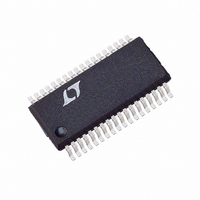
LTC1411CG#TRPBF Linear Technology, LTC1411CG#TRPBF Datasheet - Page 6

LTC1411CG#TRPBF
Manufacturer Part Number
LTC1411CG#TRPBF
Description
IC A/D CONV 14BIT 2.5MSPS 36SSOP
Manufacturer
Linear Technology
Datasheet
1.LTC1411IG.pdf
(16 pages)
Specifications of LTC1411CG#TRPBF
Number Of Bits
14
Sampling Rate (per Second)
2.5M
Data Interface
Parallel
Number Of Converters
1
Power Dissipation (max)
325mW
Voltage Supply Source
Analog and Digital
Operating Temperature
0°C ~ 70°C
Mounting Type
Surface Mount
Package / Case
36-SSOP (0.200", 5.30mm Width)
Lead Free Status / RoHS Status
Lead free / RoHS Compliant
TYPICAL PERFOR A CE CHARACTERISTICS
PI FU CTIO S
A
difference voltage between A
mable input ranges of 1.8V, 1.27V, 0.9V and 0.64V
depending on PGA selection. A
range between 0V and V
A
to the REFOUT pin of the ADC or tied to an external DC
voltage. This voltage is also the bipolar zero for the ADC.
A
REFOUT (Pin 3): 2.5V Reference Output. Bypass to AGND1
with a 22 F tantalum capacitor if REFOUT is tied to A
No capacitor is needed if the external reference is used to
drive A
REFIN (Pin 4): Reference Buffer Input. This pin can be
tied to REFOUT or to an external reference if more
precision is required.
REFCOM1 (Pin 5): Noise Reduction Pin. Put a 10 F
bypass capacitor at this pin to reduce the noise going into
the reference buffer.
REFCOM2 (Pin 6): 4.05V Reference Compensation Pin.
Bypass to AGND1 with a 10 F tantalum capacitor in
parallel with a 0.1 F ceramic.
LTC1411
6
IN
IN
IN
U
+
–
–
(Pin 1): Positive Analog Input. The ADC converts the
has common mode range between 0V and V
(Pin 2): Negative Analog Input. This pin can be tied
IN
–
.
U
–100
–120
–140
–20
–40
–60
–80
0
0
4096 Points FFT Plot (1MHz)
U
SINAD = 75dB
SFDR = 81dB
f
f
SAMPLE
IN
= 1MHz
250
DD
= 2.5MHz
W
.
FREQUENCY (kHz)
IN
500
+
IN
and A
U
+
750
has common mode
IN
–
1000
with program-
1411 G15
1250
DD
.
IN
–
.
AGND (Pins 7 to 9): Analog Ground. AGND1 is the ground
for the reference. AGND2 is the ground for the comparator
and AGND3 is the ground for the remaining analog
circuitry.
AVP (Pin 10): 5V Analog Power Supply. Bypass to AGND
with a 10 F tantalum capacitor.
AVM (Pin 11): Analog and Digital Substrate Pin. Tie this
pin to AGND.
D13 to D0 (Pins 12 to 25): Digital Data Outputs. D13 is the
MSB (Most Significant Bit).
OTR (Pin 26): Out-of-the-Range Pin. This pin can be used
in conjunction with D13 to determine if a signal is less than
or greater than the analog input range. If D13 is low and
OTR is high, the analog input to the ADC exceeds the
maximum voltage of the input range.
BUSY (Pin 27): Busy Output. Converter status pin. It is
low during conversion.
OGND (Pin 28): Digital Ground for Output Drivers (Data
Bits, OTR and BUSY).
OV
Drivers (Data Bits, OTR and BUSY). Bypass to OGND with
a 10 F tantalum capacitor.
DD
0.01
100
(Pin 29): 3V or 5V Digital Power Supply for Output
0.1
10
1
1
Acquisition Time
vs Source Resistance
10
SOURCE RESISTANCE ( )
100
1000
10000
1411 G16
100000
1411f


