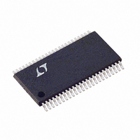
LTC1750IFW Linear Technology, LTC1750IFW Datasheet - Page 9

LTC1750IFW
Manufacturer Part Number
LTC1750IFW
Description
IC ADC 14BIT 80MSPS SMPL 48TSSOP
Manufacturer
Linear Technology
Datasheet
1.LTC1750CFW.pdf
(20 pages)
Specifications of LTC1750IFW
Number Of Bits
14
Sampling Rate (per Second)
80M
Data Interface
Parallel
Number Of Converters
1
Power Dissipation (max)
1.69W
Voltage Supply Source
Single Supply
Operating Temperature
-40°C ~ 85°C
Mounting Type
Surface Mount
Package / Case
48-TFSOP (0.240", 6.10mm Width)
Lead Free Status / RoHS Status
Contains lead / RoHS non-compliant
Available stocks
Company
Part Number
Manufacturer
Quantity
Price
Part Number:
LTC1750IFW#PBF
Manufacturer:
LINEAR/凌特
Quantity:
20 000
SENSE (Pin 1): Reference Sense Pin. GND selects a V
of 0.7V. V
and 1.125V, V
is V
V
Bypass to ground with 4.7 F ceramic chip capacitor.
GND (Pins 3, 6, 9, 12, 13, 16, 19, 21, 36, 37): ADC Power
Ground.
A
A
V
with 1 F ceramic chip capacitors at Pin 8 and Pin 18.
REFLB (Pin 10): ADC Low Reference. Bypass to Pin 11
with 0.1 F ceramic chip capacitor. Do not connect to
Pin 14.
REFHA (Pin 11): ADC High Reference. Bypass to Pin 10 with
0.1 F ceramic chip capacitor, to Pin 14 with a 4.7 F ceramic
capacitor and to ground with 1 F ceramic capacitor.
REFLA (Pin 14): ADC Low Reference. Bypass to Pin 15 with
0.1 F ceramic chip capacitor, to Pin 11 with a 4.7 F ce-
ramic capacitor and to ground with 1 F ceramic capacitor.
REFHB (Pin 15): ADC High Reference. Bypass to Pin 14
with 0.1 F ceramic chip capacitor. Do not connect to
Pin 11.
PI FU CTIO S
CM
IN
IN
DD
U
+
–
(Pins 7, 8, 17, 18, 20): 5V Supply. Bypass to AGND
(Pin 2): 2.0V Output and Input Common Mode Bias.
(Pin 4): Positive Differential Analog Input.
(Pin 5): Negative Differential Analog Input.
REF
/PGA gain.
DD
U
selects 1.125V. When V
SENSE
is used as V
U
REF
. The ADC input range
SENSE
is between 0.7V
REF
MSBINV (Pin 22): MSB Inversion Control. Low inverts the
MSB, 2’s complement output format. High does not invert
the MSB, offset binary output format.
ENC (Pin 23): Encode Input. The input sample starts on the
positive edge.
ENC (Pin 24): Encode Complement Input. Conversion
starts on the negative edge. Bypass to ground with 0.1 F
ceramic for single-ended ENCODE signal.
PGA (Pin 25): Programmable Gain Amplifier Control. Low
selects an effective front-end gain of 1. High selects an
effective gain of 1 2/3. The ADC input range is V
gain.
CLKOUT (Pin 26): Data Valid Output. Latch data on the
rising edge of CLKOUT.
OGND (Pins 27, 38, 47): Output Driver Ground.
D0-D3 (Pins 28 to 31): Digital Outputs.
OV
ers. Bypass to ground with 0.1 F ceramic chip capacitor.
D4-D6 (Pins 33 to 35): Digital Outputs.
D7-D10 (Pins 39 to 42): Digital Outputs.
D11-D13 (Pins 44 to 46): Digital Outputs.
OF (Pin 48): Over/Under Flow Output. High when an over
or under flow has occurred.
DD
(Pins 32, 43): Positive Supply for the Output Driv-
LTC1750
REF
/PGA
9
1750f


