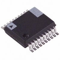
AD9057BRSZ-RL40 Analog Devices Inc, AD9057BRSZ-RL40 Datasheet - Page 3

AD9057BRSZ-RL40
Manufacturer Part Number
AD9057BRSZ-RL40
Description
IC ADC 8BIT 40MSPS 20-SSOP T/R
Manufacturer
Analog Devices Inc
Datasheet
1.AD9057BRSZ-RL40.pdf
(12 pages)
Specifications of AD9057BRSZ-RL40
Number Of Bits
8
Sampling Rate (per Second)
40M
Data Interface
Parallel
Number Of Converters
1
Power Dissipation (max)
260mW
Voltage Supply Source
Analog and Digital
Operating Temperature
-40°C ~ 85°C
Mounting Type
Surface Mount
Package / Case
20-SSOP (0.200", 5.30mm Width)
Lead Free Status / RoHS Status
Lead free / RoHS Compliant
Parameter
DIGITAL OUTPUTS
POWER SUPPLY
NOTES
1
2
3
4
5
6
Specifications subject to change without notice.
REV. D
Gain error and gain temperature coefficient are based on the ADC only (with a fixed 2.5 V external reference).
t
SNR/harmonics based on an analog input voltage of –0.5 dBFS referenced to a 1.0 V full-scale input range.
Digital supply current based on V
Power dissipation is based on specified encode and 10.3 MHz analog input dynamic test conditions (V
Typical thermal impedance for the RS style (SSOP) 20-lead package : q
an ac load of 10 pF or a dc current of ± 40 mA.
V
Logic 1 Voltage (V
Logic 1 Voltage (V
Logic 0 Voltage
Output Coding
V
V
Power Dissipation
Power-Down Dissipation
Power Supply Rejection Ratio
and t
D
DD
(PSRR)
Supply Current (V
Supply Current (V
PD
are measured from the 1.5 V level of the encode to the 10%/90% levels of the digital output swing. The digital output load during test is not to exceed
DD
DD
5, 6
= 3 V)
= 5 V)
D
DD
= 5 V)
= 3 V)
DD
OUTPUTS
= 3 V output drive with <10 pF loading under dynamic test conditions.
ENCODE
DIGITAL
4
EXPLANATION OF TEST LEVELS
Test Level
I
II
III
IV
V
VI
AIN
Temp
Full
Full
Full
Full
Full
Full
25∞C
Full
N
t
EH
t
A
t
t
t
t
t
Test
Level
VI
IV
VI
VI
VI
VI
VI
V
N – 3
A
EH
EL
V
PD
Description
100% production tested.
100% production tested at 25∞C and sample
tested at specified temperatures.
Sample tested only.
Parameter is guaranteed by design and charac-
terization testing.
Parameter is a typical value only.
100% production tested at 25∞C; guaranteed
by design and characterization testing
for industrial temperature range.
APERTURE DELAY
PULSEWIDTH HIGH
PULSEWIDTH LOW
OUTPUT VALID TIME
OUTPUT PROP DELAY
Figure 1. Timing Diagram
N + 1
2.95
4.95
Offset Binary Code
N – 2
Min
t
AD9057BRS-40
EL
JC
= 46∞C/W, q
N + 2
Typ
36
4.0
192
6
3
N – 1
–3–
4.0 ns
CA
MIN
0.05
48
6.5
260
10
Max
N + 3
= 80∞C/W, and q
t
V
t
PD
N
TYP
2.7 ns
6.6 ns
9.5 ns
Min
2.95
4.95
Offset Binary Code
AD9057BRS-60
N + 4
MAX
166 ns
166 ns
D
N + 1
= 5 V ± 5%, V
JA
38
Typ
5.5
205
6
3
= 126∞C/W.
N + 5
N + 2
Max
0.05
48
6.5
260
10
DD
= 3 V ± 5%).
Min
2.95
4.95
Offset Binary Code
AD9057BRS-80
Typ
40
7.4
220
6
3
Max
0.05
51
8.8
281
10
AD9057
Unit
V
V
V
mA
mA
mW
mW
mV/V


