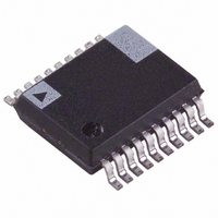
AD9057BRSZ-RL40 Analog Devices Inc, AD9057BRSZ-RL40 Datasheet - Page 8

AD9057BRSZ-RL40
Manufacturer Part Number
AD9057BRSZ-RL40
Description
IC ADC 8BIT 40MSPS 20-SSOP T/R
Manufacturer
Analog Devices Inc
Datasheet
1.AD9057BRSZ-RL40.pdf
(12 pages)
Specifications of AD9057BRSZ-RL40
Number Of Bits
8
Sampling Rate (per Second)
40M
Data Interface
Parallel
Number Of Converters
1
Power Dissipation (max)
260mW
Voltage Supply Source
Analog and Digital
Operating Temperature
-40°C ~ 85°C
Mounting Type
Surface Mount
Package / Case
20-SSOP (0.200", 5.30mm Width)
Lead Free Status / RoHS Status
Lead free / RoHS Compliant
AD9057
The AD9057 provides high impedance digital output operation
when the ADC is driven into power-down mode (PWRDN, logic
high). A 200 ns (minimum) power-down time should be
provided before a high impedance characteristic is required at
the outputs. A 200 ns power-up period should be provided to
ensure accurate ADC output data after reactivation (valid out-
put data is available three clock cycles after the 200 ns delay).
Timing
The AD9057 is guaranteed to operate with conversion rates from
5 MSPS to 80 MSPS depending on grade. The ADC is designed
to operate with an encode duty cycle of 50%, but performance
is insensitive to moderate variations. Pulsewidth variations of
up to ± 10% (allowing the encode signal to meet the minimum/
maximum high/low specifications) will cause no degradation in
ADC performance (see Figure 1 timing diagram).
Power Dissipation
The power dissipation of the AD9057 is specified to reflect a
typical application setup under the following conditions: analog
input is –0.5 dBFS at 10.3 MHz, V
outputs are loaded with 7 pF typical (10 pF maximum). The
actual dissipation will vary as these conditions are modified in
user applications. TPC 7 shows typical power consumption for the
AD9057 versus ADC encode frequency and V
A power-down function allows users to reduce power dissipation
when ADC data is not required. A TTL/CMOS high signal
(PWRDN) shuts down portions of the ADC and brings total
power dissipation to less than 10 mW. The internal band gap
voltage reference remains active during power-down mode to
minimize ADC reactivation time. If the power-down function is
not desired, Pin 1 should be tied to ground.
APPLICATIONS
The wide analog bandwidth of the AD9057 makes it attractive for
a variety of high performance receiver and encoder applications.
Figure 4 shows two ADCs in a typical low cost I and Q demodula-
tor implementation for cable, satellite, or wireless LAN modem
receivers. The excellent dynamic performance of the ADC at
higher analog input frequencies and encode rates empowers
users to employ direct IF sampling techniques (refer to TPC 2
spectral plot). IF sampling eliminates or simplifies analog mixer
and filter stages to reduce total system cost and power.
The high sampling rate and analog bandwidth of the AD9057
are ideal for computer RGB video digitizer applications. With a
IF IN
Figure 4. I and Q Digital Receiver
VCO
90
BPF
BPF
D
is 5 V, V
AD9057
AD9057
VCO
DD
DD
is 3 V, and digital
supply voltage.
–8–
full-power analog bandwidth of 2¥ the maximum sampling rate,
the ADC provides sufficient pixel-to-pixel transient settling time
to ensure accurate 60 MSPS video digitization. Figure 5 shows a
typical RGB video digitizer implementation for the AD9057.
Evaluation Board
The AD9057/PCB evaluation board provides an easy-to-use
analog/digital interface for the 8-bit, 60 MSPS ADC. The board
includes typical hardware configurations for a variety of high
speed digitization evaluations. On-board components include
the AD9057 (in the 20-lead SSOP package), an optional analog
input buffer amplifier, a digital output latch, board timing drivers,
an analog reconstruction digital-to-analog converter, and config-
urable jumpers for ac coupling, dc coupling, and power-down
function testing. The board is configured at shipment for dc
coupling using the AD9057’s internal voltage reference.
For dc-coupled analog input applications, amplifier U2 is con-
figured to operate as a unity gain inverter with adjustable offset
for the analog input signal. For full-scale ADC drive, the analog
input signal should be 1 V p-p into 50 W (R1) referenced to
ground (0 V). The amplifier offsets the analog signal by +VREF
(2.5 V typical) to center the voltage for proper ADC input drive.
For dc-coupled operation, connect E1 to E2 (analog input to
R2) and E11 to E12 (amplifier output to analog input of AD9057)
using the board jumper connectors. DC offset of the analog
input signal can be modified by adjusting potentiometer R10.
For ac-coupled analog input applications, amplifier U2 is
removed from the analog signal path. The analog signal is
coupled into the input of the AD9057 through capacitor C2.
The ADC pulls analog input bias current from the VREF IN
voltage through the 1 kW resistor internal to the AD9057 (BIAS
OUT). The analog input signal to the board should be 1 V p-p
into 50 W (R1) for full-scale ADC drive. For ac-coupled operation,
connect E1 to E3 (analog input A to C2 feedthrough capacitor)
and E10 to E12 (C2 to the analog input and internal bias resis-
tor) using the board jumper connectors.
The on-board reference voltage may be used to drive the ADC
or an external reference may be applied. To use the internal
voltage reference, connect E6 to E5 (VREF OUT to VREF IN).
To apply an external voltage reference, connect E4 to E5
(external reference from the REF banana jack to VREF IN).
The external voltage reference should be 2.5 V ± 10%.
H-SYNC
GREEN
BLUE
RED
Figure 5. RGB Video Encoder
AD9057
AD9057
AD9057
PLL
PIXEL CLOCK
8
8
8
REV. D


