CS5345-CQZR Cirrus Logic Inc, CS5345-CQZR Datasheet - Page 28
CS5345-CQZR
Manufacturer Part Number
CS5345-CQZR
Description
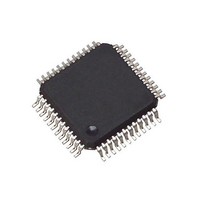
IC ADC AUD 105DB 200KHZ 48-LQFP
Manufacturer
Cirrus Logic Inc
Datasheet
1.CS5345-CQZ.pdf
(41 pages)
Specifications of CS5345-CQZR
Package / Case
48-LQFP
Number Of Bits
24
Sampling Rate (per Second)
200k
Data Interface
Serial
Number Of Converters
2
Power Dissipation (max)
485mW
Voltage Supply Source
Analog and Digital
Operating Temperature
-10°C ~ 70°C
Mounting Type
Surface Mount
Conversion Rate
192 KSPs
Resolution
24 bit
Number Of Adc Inputs
6
Operating Supply Voltage
5 V
Maximum Operating Temperature
+ 70 C
Minimum Operating Temperature
- 10 C
Mounting Style
SMD/SMT
Supply Voltage (max)
5.25 V
Supply Voltage (min)
3.13 V
Lead Free Status / RoHS Status
Lead free / RoHS Compliant
For Use With
598-1780 - EVALUATION BOARD FOR CS5345
Lead Free Status / RoHS Status
Lead free / RoHS Compliant, Lead free / RoHS Compliant
Available stocks
Company
Part Number
Manufacturer
Quantity
Price
Company:

Part Number:
CS5345-CQZR
Manufacturer:
Cirrus Logic Inc
Quantity:
10 000


28
4.8
4.9
4.10
4.11
Interrupts and Overflow
The CS5345 has a comprehensive interrupt capability. The INT output pin is intended to drive the interrupt
input pin on the host microcontroller. The INT pin may function as either an active high CMOS driver or an
active low open-drain driver (see
open-drain, the INT pin has no active pull-up transistor, allowing it to be used for wired-OR hook-ups with
multiple peripherals connected to the microcontroller interrupt input pin. In this configuration, an external
pull-up resistor must be placed on the INT pin for proper operation.
Many conditions can cause an interrupt, as listed in the interrupt status register descriptions (see
Status - Address 0Dh” on page
each source may be set to rising edge, falling edge, or level-sensitive. Combined with the option of level-
sensitive or edge-sensitive modes within the microcontroller, many different configurations are possible, de-
pending on the needs of the equipment designer.
The CS5345 also has a dedicated overflow output. The OVFL pin functions as active low open drain and
has no active pull-up transistor, thereby requiring an external pull-up resistor. The OVFL pin outputs an OR
of the ADCOverflow and ADCUnderflow conditions available in the Interrupt Status register; however, these
conditions do not need to be unmasked for proper operation of the OVFL pin.
Reset
When RESET is low, the CS5345 enters a low-power mode and all internal states are reset, including the
control port and registers, the outputs are muted. When RESET is high, the control port becomes operation-
al, and the desired settings should be loaded into the control registers. Writing a 0 to the PDN bit in the Pow-
er Control register will then cause the part to leave the low-power state and begin operation.
The delta-sigma modulators settle in a matter of microseconds after the analog section is powered, either
through the application of power or by setting the RESET pin high. However, the voltage reference will take
much longer to reach a final value due to the presence of external capacitance on the FILT+ pin. During this
voltage reference ramp delay, SDOUT will be automatically muted.
It is recommended that RESET be activated if the analog or digital supplies drop below the recommended
operating condition to prevent power-glitch-related issues.
Synchronization of Multiple Devices
In systems where multiple ADCs are required, care must be taken to achieve simultaneous sampling. To
ensure synchronous sampling, the master clocks and left/right clocks must be the same for all of the
CS5345s in the system. If only one master clock source is needed, one solution is to place one CS5345 in
Master Mode, and slave all of the other CS5345s to the one master. If multiple master clock sources are
needed, a possible solution would be to supply all clocks from the same external source and time the
CS5345 reset with the inactive edge of master clock. This will ensure that all converters begin sampling on
the same clock edge.
Grounding and Power Supply Decoupling
As with any high-resolution converter, the CS5345 requires careful attention to power supply and grounding
arrangements if its potential performance is to be realized.
rangements, with VA connected to a clean supply. VD, which powers the digital filter, may be run from the
Receive byte, contents of selected register.
Send acknowledge bit.
Send stop condition.
35). Each source may be masked off through mask register bits. In addition,
“Active High/Low (Bit 0)” on page
Figure 7
35). When configured as active low
shows the recommended power ar-
CS5345
DS658F2
“Interrupt
Related parts for CS5345-CQZR
Image
Part Number
Description
Manufacturer
Datasheet
Request
R

Part Number:
Description:
IC ADC AUD 104DB 200KHZ 48-LQFP
Manufacturer:
Cirrus Logic Inc
Datasheet:

Part Number:
Description:
IC,Data Acquisition Signal Conditioner,6-CHANNEL,24-BIT,CMOS,QFP,48PIN,PLASTIC
Manufacturer:
Cirrus Logic Inc
Datasheet:
Part Number:
Description:
IC,Data Acquisition Signal Conditioner,6-CHANNEL,24-BIT,CMOS,QFP,48PIN,PLASTIC
Manufacturer:
Cirrus Logic Inc
Datasheet:

Part Number:
Description:
Fast Recovery High Voltage Silicon Rectifiers
Manufacturer:
Fuji Electric holdings CO.,Ltd
Datasheet:

Part Number:
Description:
Fast Recovery High Voltage Silicon Rectifiers
Manufacturer:
Fuji Electric
Datasheet:
Part Number:
Description:
RF COILS < SMD Type: CS Series>
Manufacturer:
SUMIDA [Sumida Corporation]
Datasheet:
Part Number:
Description:
Fast Recovery High Voltage Silicon Rectifiers
Manufacturer:
FUJI [Fuji Electric]
Datasheet:
Part Number:
Description:
Development Kit
Manufacturer:
Cirrus Logic Inc
Datasheet:
Part Number:
Description:
Development Kit
Manufacturer:
Cirrus Logic Inc
Datasheet:


Part Number:
Description:
High-efficiency PFC + Fluorescent Lamp Driver Reference Design
Manufacturer:
Cirrus Logic Inc
Datasheet:
Part Number:
Description:
Development Kit
Manufacturer:
Cirrus Logic Inc
Datasheet:
Part Number:
Description:
Development Kit
Manufacturer:
Cirrus Logic Inc
Datasheet:

Part Number:
Description:
Development Kit
Manufacturer:
Cirrus Logic Inc
Datasheet:

Part Number:
Description:
Ref Bd For Speakerbar MSA & DSP Products
Manufacturer:
Cirrus Logic Inc