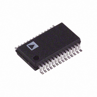
AD9200JRSZ Analog Devices Inc, AD9200JRSZ Datasheet - Page 3

AD9200JRSZ
Manufacturer Part Number
AD9200JRSZ
Description
IC ADC 10BIT CMOS 20MSPS 28-SSOP
Manufacturer
Analog Devices Inc
Datasheet
1.AD9200ARSZRL.pdf
(24 pages)
Specifications of AD9200JRSZ
Data Interface
Parallel
Number Of Bits
10
Sampling Rate (per Second)
20M
Number Of Converters
9
Power Dissipation (max)
100mW
Voltage Supply Source
Single Supply
Operating Temperature
0°C ~ 70°C
Mounting Type
Surface Mount
Package / Case
28-SSOP (0.200", 5.30mm Width)
Resolution (bits)
10bit
Sampling Rate
20MSPS
Input Channel Type
Differential, Single Ended
Supply Voltage Range - Analog
2.7V To 5.5V
Number Of Elements
1
Resolution
10Bit
Architecture
Pipelined
Sample Rate
20MSPS
Input Polarity
Unipolar
Input Type
Voltage
Rated Input Volt
±0.5/±1V
Differential Input
Yes
Power Supply Requirement
Analog and Digital
Single Supply Voltage (typ)
3V
Single Supply Voltage (min)
2.7V
Single Supply Voltage (max)
5.5V
Dual Supply Voltage (typ)
Not RequiredV
Dual Supply Voltage (min)
Not RequiredV
Dual Supply Voltage (max)
Not RequiredV
Power Dissipation
100mW
Differential Linearity Error
±1LSB
Integral Nonlinearity Error
±2LSB
Operating Temp Range
0C to 70C
Operating Temperature Classification
Commercial
Mounting
Surface Mount
Pin Count
28
Package Type
SSOP
Lead Free Status / RoHS Status
Lead free / RoHS Compliant
Lead Free Status / RoHS Status
Lead free / RoHS Compliant, Lead free / RoHS Compliant
Available stocks
Company
Part Number
Manufacturer
Quantity
Price
Part Number:
AD9200JRSZ
Manufacturer:
ADI/亚德诺
Quantity:
20 000
REV. E
Parameter
DIGITAL INPUTS
DIGITAL OUTPUTS
LOGIC OUTPUT (with DRVDD = 3 V)
LOGIC OUTPUT (with DRVDD = 5 V)
CLOCKING
CLAMP
NOTES
1
2
Specifications subject to change without notice.
See Figures 1a and 1b.
Available only in AD9200ARS and AD9200KST.
High Input Voltage
Low Input Voltage
High-Z Leakage
Data Valid Delay
Data Enable Delay
Data High-Z Delay
High Level Output Voltage (I
High Level Output Voltage (I
Low Level Output Voltage (I
Low Level Output Voltage (I
High Level Output Voltage (I
High Level Output Voltage (I
Low Level Output Voltage (I
Low Level Output Voltage (I
Clock Pulsewidth High
Clock Pulsewidth Low
Pipeline Latency
Clamp Error Voltage
Clamp Pulsewidth
2
OL
OL
OL
OL
OH
OH
OH
OH
AV
= 1.6 mA)
= 50 A)
= 1.6 mA)
= 50 A)
= 50 A)
= 50 A)
= 0.5 mA)
= 0.5 mA)
DD
REFTS
REFBS
MODE
10k
10k
Symbol
V
V
I
t
t
t
V
V
V
V
V
V
V
V
t
t
E
t
OD
DEN
DHZ
CH
CL
CPW
OZ
Figure 1a.
IH
IL
OH
OH
OL
OL
OH
OH
OL
OL
OC
AD9200
0.4
V
DD
Min
2.4
–10
+2.95
+2.80
+4.5
+2.4
22.5
22.5
–3–
Typ
25
25
13
3
2
20
REFTF
REFBF
Max
0.3
+10
+0.4
+0.05
+0.4
+0.1
40
REFBS
MODE
REFTS
Units
V
V
ns
ns
ns
V
V
V
V
V
V
V
V
ns
ns
Cycles
mV
A
s
Figure 1b.
4.2k
AD9200
Condition
Output = GND to VDD
C
CLAMPIN = 0.5 V–2.7 V, R
C
L
IN
= 20 pF
= 1 F (Period = 63.5 s)
AD9200
IN
= 10


