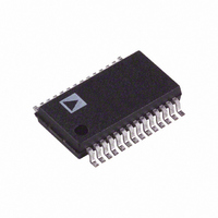
AD9200JRSZ Analog Devices Inc, AD9200JRSZ Datasheet - Page 8

AD9200JRSZ
Manufacturer Part Number
AD9200JRSZ
Description
IC ADC 10BIT CMOS 20MSPS 28-SSOP
Manufacturer
Analog Devices Inc
Datasheet
1.AD9200ARSZRL.pdf
(24 pages)
Specifications of AD9200JRSZ
Data Interface
Parallel
Number Of Bits
10
Sampling Rate (per Second)
20M
Number Of Converters
9
Power Dissipation (max)
100mW
Voltage Supply Source
Single Supply
Operating Temperature
0°C ~ 70°C
Mounting Type
Surface Mount
Package / Case
28-SSOP (0.200", 5.30mm Width)
Resolution (bits)
10bit
Sampling Rate
20MSPS
Input Channel Type
Differential, Single Ended
Supply Voltage Range - Analog
2.7V To 5.5V
Number Of Elements
1
Resolution
10Bit
Architecture
Pipelined
Sample Rate
20MSPS
Input Polarity
Unipolar
Input Type
Voltage
Rated Input Volt
±0.5/±1V
Differential Input
Yes
Power Supply Requirement
Analog and Digital
Single Supply Voltage (typ)
3V
Single Supply Voltage (min)
2.7V
Single Supply Voltage (max)
5.5V
Dual Supply Voltage (typ)
Not RequiredV
Dual Supply Voltage (min)
Not RequiredV
Dual Supply Voltage (max)
Not RequiredV
Power Dissipation
100mW
Differential Linearity Error
±1LSB
Integral Nonlinearity Error
±2LSB
Operating Temp Range
0C to 70C
Operating Temperature Classification
Commercial
Mounting
Surface Mount
Pin Count
28
Package Type
SSOP
Lead Free Status / RoHS Status
Lead free / RoHS Compliant
Lead Free Status / RoHS Status
Lead free / RoHS Compliant, Lead free / RoHS Compliant
Available stocks
Company
Part Number
Manufacturer
Quantity
Price
Part Number:
AD9200JRSZ
Manufacturer:
ADI/亚德诺
Quantity:
20 000
AD9200
Modes
TOP/BOTTOM
CENTER SPAN AIN
Differential
External Ref
AD876
Figure 14. Input Bias Current vs. Input Voltage
–12
–15
–18
–21
–24
–27
–25
–10
–15
–20
–3
–6
–9
1.0E+6
25
20
15
10
–5
0
5
0
0
Figure 13. Full Power Bandwidth
0.5
Input
Connect
AIN
AIN
AIN
AIN Is Input 1
REFTS and
REFBS Are
Shorted Together
for Input 2
AIN
AIN
10.0E+6
1.0
INPUT VOLTAGE – V
FREQUENCY – Hz
1.5
Input
Span
1 V
2 V
1 V
2 V
1 V
2 V
2 V max AVDD
2 V
100.0E+6
2.0
REFBS = 0.5V
REFTS = 2.5V
CLOCK = 20MHz
MODE
Pin
AVDD
AVDD
AVDD/2 Short VREF and REFSENSE Together
AVDD/2 AGND
AVDD/2 Short VREF and REFSENSE Together
AVDD/2 AGND
AGND
Float or
AVSS
2.5
1.0E+9
Table I. Mode Selection
3.0
REFSENSE
Pin
Short REFSENSE, REFTS and VREF Together
AGND
AVDD
AVDD
–8–
APPLYING THE AD9200
THEORY OF OPERATION
The AD9200 implements a pipelined multistage architecture to
achieve high sample rate with low power. The AD9200 distrib-
utes the conversion over several smaller A/D subblocks, refining
the conversion with progressively higher accuracy as it passes
the results from stage to stage. As a consequence of the distrib-
uted conversion, the AD9200 requires a small fraction of the
1023 comparators used in a traditional flash type A/D. A
sample-and-hold function within each of the stages permits the
first stage to operate on a new input sample while the second,
third and fourth stages operate on the three preceding samples.
OPERATIONAL MODES
The AD9200 is designed to allow optimal performance in a
wide variety of imaging, communications and instrumentation
applications, including pin compatibility with the AD876 A/D.
To realize this flexibility, internal switches on the AD9200 are
used to reconfigure the circuit into different modes. These modes
are selected by appropriate pin strapping. There are three parts
of the circuit affected by this modality: the voltage reference, the
reference buffer, and the analog input. The nature of the appli-
cation will determine which mode is appropriate: the descrip-
tions in the following sections, as well as the Table I should
assist in picking the desired mode.
REF
Short REFTS and VREF Together
No Connect
No Connect
No Connect
No Connect
REFTS
AVDD/2
AVDD/2
AVDD/2
AVDD/2
Span = REFTS
– REFBS (2 V max)
Short to
VREFTF
Short to
VREFTF
REFBS
AGND
AGND
AVDD/2
AVDD/2
AVDD/2
AVDD/2
Short to
VREFBF
Short to
VREFBF
Figure
18
19
20
29
21, 22
23
30
REV. E


