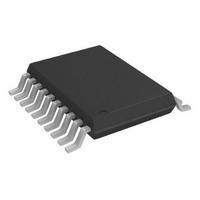
AD7927BRUZ Analog Devices Inc, AD7927BRUZ Datasheet - Page 13

AD7927BRUZ
Manufacturer Part Number
AD7927BRUZ
Description
IC ADC 12BIT 8CH 200KSPS 20TSSOP
Manufacturer
Analog Devices Inc
Specifications of AD7927BRUZ
Data Interface
DSP, MICROWIRE™, QSPI™, Serial, SPI™
Number Of Bits
12
Sampling Rate (per Second)
200k
Number Of Converters
1
Power Dissipation (max)
7.5mW
Voltage Supply Source
Single Supply
Operating Temperature
-40°C ~ 85°C
Mounting Type
Surface Mount
Package / Case
20-TSSOP (0.173", 4.40mm Width)
Resolution (bits)
12bit
Sampling Rate
200kSPS
Input Channel Type
Single Ended
Supply Voltage Range - Analog
2.7V To 5.25V
Supply Current
1.5mA
Number Of Elements
1
Resolution
12Bit
Architecture
SAR
Sample Rate
200KSPS
Input Polarity
Unipolar
Input Type
Voltage
Rated Input Volt
2.5/5V
Differential Input
No
Power Supply Requirement
Analog and Digital
Single Supply Voltage (typ)
3/5V
Single Supply Voltage (min)
2.7V
Single Supply Voltage (max)
5.25V
Dual Supply Voltage (typ)
Not RequiredV
Dual Supply Voltage (min)
Not RequiredV
Dual Supply Voltage (max)
Not RequiredV
Power Dissipation
7.5mW
Differential Linearity Error
-0.9LSB/1.5LSB
Integral Nonlinearity Error
±1LSB
Operating Temp Range
-40C to 85C
Operating Temperature Classification
Industrial
Mounting
Surface Mount
Pin Count
20
Package Type
TSSOP
Input Signal Type
Single-Ended
Lead Free Status / RoHS Status
Lead free / RoHS Compliant
For Use With
EVAL-AD7927CBZ - BOARD EVALUATION FOR AD7927
Lead Free Status / Rohs Status
Compliant
Available stocks
Company
Part Number
Manufacturer
Quantity
Price
Company:
Part Number:
AD7927BRUZ
Manufacturer:
ADI
Quantity:
1 000
Part Number:
AD7927BRUZ
Manufacturer:
ADI/亚德诺
Quantity:
20 000
Company:
Part Number:
AD7927BRUZ-REEL7
Manufacturer:
ADI
Quantity:
3
Company:
Part Number:
AD7927BRUZ-REEL7
Manufacturer:
ADI
Quantity:
1 000
ADC TRANSFER FUNCTION
The output coding of the AD7927 is either straight binary or
twos complement, depending on the status of the LSB in the
Control Register. The designed code transitions occur at suc-
cessive LSB values (i.e., 1 LSB, 2 LSBs, and so forth). The LSB
Handling Bipolar Input Signals
Figure 10 shows how useful the combination of the 2 ¥ REF
input range and the twos complement output coding scheme is
for handling bipolar input signals. If the bipolar input signal is
biased about REF
selected, then REF
negative full scale and +REF
a dynamic range of 2 ¥ REF
TYPICAL CONNECTION DIAGRAM
Figure 11 shows a typical connection diagram for the AD7927.
In this setup, the AGND pin is connected to the analog ground
plane of the system. In Figure 11, REF
decoupled 2.5 V supply from a reference source, the AD780, to
provide an analog input range of 0 V to 2.5 V (if RANGE bit is 1)
or 0 V to 5 V (if RANGE bit is 0). Although the AD7927 is con-
nected to a AV
microprocessor. The V
the same 3 V supply of the microprocessor to allow a 3 V logic
interface (see the Digital Inputs section). The conversion result is
output in a 16-bit word. This 16-bit data stream consists of one
REV. 0
Figure 8. Straight Binary Transfer Characteristic
111…111
111…110
111…000
011…111
000…010
000…001
000…000
•
•
•
•
•
DD
NOTE: V
of 5 V, the serial interface is connected to a 3 V
IN
IN
0V
and twos complement output coding is
0V
REF
becomes the zero code point, –REF
V
1 LSB
DRIVE
IS EITHER REF
IN
pin of the AD7927 is connected to
IN
ANALOG INPUT
.
becomes positive full scale, with
1LSB
IN
OR 2
V
REF
IN
+V
V
/4096
is connected to a
REF
REF
0.1 F
R3
R2
IN
1 LSB
Figure 10. Handling Bipolar Signals
R1
R2
V
REF
R4
R1
R3
IN
R4
is
IN
–13–
REF
V
V
IN
IN
0
7
AD7927
IN
size is REF
teristic for the AD7927 when straight binary coding is selected
is shown in Figure 8, and the ideal transfer characteristic for the
AD7927 when twos complement coding is selected is shown in
Figure 9.
Figure 9. Twos Complement Transfer Characteristic with
REF
leading zero, three address bits indicating which channel the
conversion result corresponds to, followed by the 12 bits of
conversion data. For applications where power consumption is
of concern, the power-down modes should be used between
conversions or bursts of several conversions to improve power
performance. (See the Modes of Operation section.)
AV
DD
0V TO REF
V
IN
DOUT
DRIVE
NOTE: ALL UNUSED INPUT CHANNELS SHOULD BE CONNECTED TO AGND
± REF
0.1 F
IN
Figure 11. Typical Connection Diagram
IN
COMPLEMENT
+REF
–REF
IN
/4096 for the AD7927. The ideal transfer charac-
011…111
011…110
000…001
000…000
111…111
100…010
100…001
100…000
V
AGND
V
REF
IN
IN
TWOS
Input Range
7
0
•
•
•
•
•
•
IN
IN
IN
AV
REF
DD
–V
(= 2
(= 0V)
0.1 F
REF
IN
AD7927
REF
DSP/ P
AD780
1LSB
V
2.5V
V
DD
DD
IN
10 F
)
V
REF
ANALOG INPUT
V
1LSB
DRIVE
1LSB
011…111
000…000
100…000
SCLK
DOUT
0.1 F
SUPPLY
+V
DIN
CS
REF
2
5V
V
REF
1LSB
10 F
INTERFACE
4096
SERIAL
AD7927
SUPPLY
C/ P
3V


