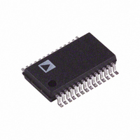
AD9201ARS Analog Devices Inc, AD9201ARS Datasheet - Page 10

AD9201ARS
Manufacturer Part Number
AD9201ARS
Description
IC ADC CMOS 10BIT DUAL 28-SSOP
Manufacturer
Analog Devices Inc
Specifications of AD9201ARS
Mounting Type
Surface Mount
Rohs Status
RoHS non-compliant
Number Of Bits
10
Sampling Rate (per Second)
20M
Data Interface
Parallel
Number Of Converters
2
Power Dissipation (max)
245mW
Voltage Supply Source
Analog and Digital
Operating Temperature
-40°C ~ 85°C
Package / Case
28-SSOP (0.200", 5.30mm Width)
Input Channels Per Adc
2
No. Of Channels
2
Peak Reflow Compatible (260 C)
No
Inl ±
2.5LSB
Sample Rate
20MSPS
No. Of Bits
10 Bit
Leaded Process Compatible
No
Dnl±
1LSB
Number Of Elements
2
Resolution
10Bit
Architecture
Pipelined
Input Polarity
Unipolar
Input Type
Voltage
Rated Input Volt
1.5V
Differential Input
Yes
Power Supply Requirement
Analog and Digital
Single Supply Voltage (typ)
3V
Single Supply Voltage (min)
2.7V
Single Supply Voltage (max)
5.5V
Dual Supply Voltage (typ)
Not RequiredV
Dual Supply Voltage (min)
Not RequiredV
Dual Supply Voltage (max)
Not RequiredV
Differential Linearity Error
±1LSB
Integral Nonlinearity Error
±2.5LSB
Operating Temp Range
-40C to 85C
Operating Temperature Classification
Industrial
Mounting
Surface Mount
Pin Count
28
Package Type
SSOP
Lead Free Status / Rohs Status
Not Compliant
Available stocks
Company
Part Number
Manufacturer
Quantity
Price
Part Number:
AD9201ARS
Manufacturer:
ADI/亚德诺
Quantity:
20 000
Part Number:
AD9201ARSZ
Manufacturer:
ADI/亚德诺
Quantity:
20 000
Company:
Part Number:
AD9201ARSZ-REEL
Manufacturer:
SIEMENS
Quantity:
3
AD9201
REFERENCE AND REFERENCE BUFFER
The reference and buffer circuitry on the AD9201 is configured
for maximum convenience and flexibility. An illustration of the
equivalent reference circuit is show in Figure 26. The user can
select from five different reference modes through appropriate
pin-strapping (see Table I below). These pin strapping options
cause the internal circuitry to reconfigure itself for the appropri-
ate operating mode.
Mode
1 V
2 V
Programmable
External
1 V Mode (Figure 22)—provides a 1 V reference and 1 V input
full scale. Recommended for applications wishing to optimize
high frequency performance, or any circuit on a supply voltage
of less than 4 V. The part is placed in this mode by shorting the
REFSENSE pin to the VREF pin.
2 V Mode (Figure 23)—provides a 2 V reference and 2 V input
full scale. Recommended for noise sensitive applications on 5 V
supplies. The part is placed in 2 V reference mode by grounding
(shorting to AVSS) the REFSENSE pin.
1V
2V
0V
0V
5k
5k
10 F
10 F
10 F
10 F
Figure 22. 0 V to 1 V Input
Figure 23. 0 V to 2 V Input
Input Span
1 V
2 V
1 + (R1/R2)
= External Ref AVDD
Table I. Table of Modes
0.1 F
0.1 F
0.1 F
0.1 F
5k
5k
1V
VREF
IINA
IINB
IINA
IINB
VREF
REFSENSE
AD9201
REFSENSE
AD9201
I OR QREFB
I OR QREFT
I OR QREFB
I OR QREFT
REFSENSE Pin Figure
VREF
AGND
See Figure
QINA
QINB
QINA
QINB
0.1 F
0.1 F
1V
0V
2V
0V
10 F
10 F
0.1 F
0.1 F
0.1 F
0.1 F
22
23
24
25
–10–
Externally Set Voltage Mode (Figure 24)—this mode uses
the on-chip reference, but scales the exact reference level though
the use of an external resistor divider network. VREF is wired to
the top of the network, with the REFSENSE wired to the tap
point in the resistor divider. The reference level (and input full
scale) will be equal to 1 V
used for voltage levels from 0.7 V to 2.5 V.
External Reference Mode (Figure 25)—in this mode, the on-
chip reference is disabled, and an external reference is applied to
the VREF pin. This mode is achieved by tying the REFSENSE
pin to AVDD.
Reference Buffer—The reference buffer structure takes the
voltage on the VREF pin and level-shifts and buffers it for use
by various subblocks within the two A/D converters. The two
converters share the same reference buffer amplifier to maintain
the best possible gain match between the two converters. In the
interests of minimizing high frequency crosstalk, the buffered
references for the two converters are separately decoupled on
the IREFB, IREFT, QREFB and QREFT pins, as illustrated in
Figure 26.
REFERENCE
1V
0V
VREF = 1 + R2
EXT
1V
5k
0.1 F
1 F
R2
R1
Figure 24. Programmable Reference
10 F
R1
10 F
Figure 25. External Reference
VREF
REFSENSE
AVSS
AD9201
0.1 F
0.1 F
AVDD
5k
+
–
(R1 + R2)/R1. This method can be
+ –
I OR QREFB
1V
I OR QREFT
VREF
IINA
IINB
REFSENSE
AD9201
I OR QREFB
I OR QREFT
QINA
QINB
0.1 F
0.1 F
10 F
1V
0V
0.1 F
0.1 F
10 F
0.1 F
0.1 F
REV. D


