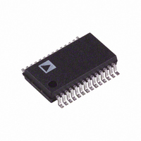
AD9201ARS Analog Devices Inc, AD9201ARS Datasheet - Page 14

AD9201ARS
Manufacturer Part Number
AD9201ARS
Description
IC ADC CMOS 10BIT DUAL 28-SSOP
Manufacturer
Analog Devices Inc
Specifications of AD9201ARS
Mounting Type
Surface Mount
Rohs Status
RoHS non-compliant
Number Of Bits
10
Sampling Rate (per Second)
20M
Data Interface
Parallel
Number Of Converters
2
Power Dissipation (max)
245mW
Voltage Supply Source
Analog and Digital
Operating Temperature
-40°C ~ 85°C
Package / Case
28-SSOP (0.200", 5.30mm Width)
Input Channels Per Adc
2
No. Of Channels
2
Peak Reflow Compatible (260 C)
No
Inl ±
2.5LSB
Sample Rate
20MSPS
No. Of Bits
10 Bit
Leaded Process Compatible
No
Dnl±
1LSB
Number Of Elements
2
Resolution
10Bit
Architecture
Pipelined
Input Polarity
Unipolar
Input Type
Voltage
Rated Input Volt
1.5V
Differential Input
Yes
Power Supply Requirement
Analog and Digital
Single Supply Voltage (typ)
3V
Single Supply Voltage (min)
2.7V
Single Supply Voltage (max)
5.5V
Dual Supply Voltage (typ)
Not RequiredV
Dual Supply Voltage (min)
Not RequiredV
Dual Supply Voltage (max)
Not RequiredV
Differential Linearity Error
±1LSB
Integral Nonlinearity Error
±2.5LSB
Operating Temp Range
-40C to 85C
Operating Temperature Classification
Industrial
Mounting
Surface Mount
Pin Count
28
Package Type
SSOP
Lead Free Status / Rohs Status
Not Compliant
Available stocks
Company
Part Number
Manufacturer
Quantity
Price
Part Number:
AD9201ARS
Manufacturer:
ADI/亚德诺
Quantity:
20 000
Part Number:
AD9201ARSZ
Manufacturer:
ADI/亚德诺
Quantity:
20 000
Company:
Part Number:
AD9201ARSZ-REEL
Manufacturer:
SIEMENS
Quantity:
3
AD9201
At the receiver, the demodulation of a QAM signal back into its
separate I and Q components is essentially the modulation pro-
cess explain above but in the reverse order. A common and
traditional implementation of a QAM demodulator is shown in
Figure 32. In this example, the demodulation is performed in
the analog domain using a dual, matched ADC and a quadra-
ture demodulator to recover and digitize the I and Q baseband
signals. The quadrature demodulator is typically a single IC
containing two mixers and the appropriate circuitry to generate
the necessary 90 phase shift between the I and Q mixers’ local
oscillators. Before being digitized by the ADCs, the mixed
down baseband I and Q signals are filtered using matched ana-
log filters. These filters, often referred to as Nyquist or Pulse-
Shaping filters, remove images-from the mixing process and any
out-of-band. The characteristics of the matching Nyquist filters
are well defined to provide optimum signal-to-noise (SNR)
performance while minimizing intersymbol interference. The
ADC’s are typically simultaneously sampling their respective
inputs at the QAM symbol rate or, most often, at a multiple of it
if a digital filter follows the ADC. Oversampling and the use of
digital filtering eases the implementation and complexity of the
analog filter. It also allows for enhanced digital processing for
both carrier and symbol recovery and tuning purposes. The use
of a dual ADC such as the AD9201 ensures excellent gain,
offset, and phase matching between the I and Q channels.
GROUNDING AND LAYOUT RULES
As is the case for any high performance device, proper ground-
ing and layout techniques are essential in achieving optimal
performance. The analog and digital grounds on the AD9201
have been separated to optimize the management of return
currents in a system. Grounds should be connected near the
ADC. It is recommended that a printed circuit board (PCB) of
at least four layers, employing a ground plane and power planes,
be used with the AD9201. The use of ground and power planes
offers distinct advantages:
1. The minimization of the loop area encompassed by a signal
2. The minimization of the impedance associated with ground
3. The inherent distributed capacitor formed by the power plane,
ASIC
DSP
and its return path.
and power paths.
PCB insulation and ground plane.
OR
Figure 32. Typical Analog QAM Demodulator
DUAL MATCHED
ADC
ADC
ADC
Q
I
FREQUENCY
NYQUIST
CARRIER
FILTERS
LO
DEMODULATOR
QUADRATURE
90°C
FROM
PREVIOUS
STAGE
–14–
These characteristics result in both a reduction of electro-
magnetic interference (EMI) and an overall improvement in
performance.
It is important to design a layout that prevents noise from cou-
pling onto the input signal. Digital signals should not be run in
parallel with the input signal traces and should be routed away
from the input circuitry. Separate analog and digital grounds
should be joined together directly under the AD9201 in a solid
ground plane. The power and ground return currents must be
carefully managed. A general rule of thumb for mixed signal
layouts dictates that the return currents from digital circuitry
should not pass through critical analog circuitry.
Transients between AVSS and DVSS will seriously degrade
performance of the ADC.
If the user cannot tie analog ground and digital ground together
at the ADC, he should consider the configuration in Figure 33.
Another input and ground technique is shown in Figure 34. A
separate ground plane has been split for RF or hard to manage
signals. These signals can be routed to the ADC differentially or
single ended (i.e., both can either be connected to the driver or
RF ground). The ADC will perform well with several hundred
mV of noise or signals between the RF and ADC analog ground.
V
IN
A
D
A
Figure 33. Ground and Power Consideration
= ANALOG
= DIGITAL
GROUND
RF
ADC
A
IC
Figure 34. RF Ground Scheme
CIRCUITS
ANALOG
AVDD
A
A
AVSS
I
A
C
C
STRAY
STRAY
ANALOG
GROUND
A
CIRCUITS
DIGITAL
DVDD
A
AIN
BIN
B
DVSS
I
ADC
D
GROUND
DATA
DIGITAL
V
D
LOGIC
DIGITAL
SUPPLY
LOGIC
LOGIC
GND
ICs
REV. D
D
-


