AD7715ANZ-3 Analog Devices Inc, AD7715ANZ-3 Datasheet - Page 7
AD7715ANZ-3
Manufacturer Part Number
AD7715ANZ-3
Description
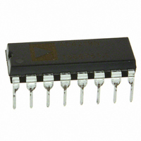
IC ADC 16BIT SIGMA-DELTA 16DIP
Manufacturer
Analog Devices Inc
Specifications of AD7715ANZ-3
Data Interface
DSP, MICROWIRE™, QSPI™, Serial, SPI™
Number Of Bits
16
Sampling Rate (per Second)
500
Number Of Converters
1
Power Dissipation (max)
9.5mW
Voltage Supply Source
Analog and Digital
Operating Temperature
-40°C ~ 85°C
Mounting Type
Through Hole
Package / Case
16-DIP (0.300", 7.62mm)
Resolution (bits)
16bit
Input Channel Type
Differential
Supply Voltage Range - Analogue
3V To 3.6V
Supply Voltage Range - Digital
3V To 5.25V
Supply Current
600µA
No. Of
RoHS Compliant
Sampling Rate
19.2kSPS
Rohs Compliant
Yes
Lead Free Status / RoHS Status
Lead free / RoHS Compliant
For Use With
EVAL-AD7715-3EBZ - BOARD EVALUATION FOR AD7715
Lead Free Status / RoHS Status
Lead free / RoHS Compliant
Available stocks
Company
Part Number
Manufacturer
Quantity
Price
Company:

Part Number:
AD7715ANZ-3
Manufacturer:
INFINEON
Quantity:
12
Part Number:
AD7715ANZ-3
Manufacturer:
ADI/亚德诺
Quantity:
20 000


REV. C
Pin No.
1
2
3
4
5
6
7
8
9
10
11
12
13
14
15
16
Mnemonic
SCLK
MCLK IN
MCLK OUT
CS
RESET
AV
AIN(+)
AIN(–)
REF IN(+)
REF IN(–)
AGND
DRDY
DOUT
DIN
DV
DGND
DD
DD
Function
Serial Clock. Logic Input. An external serial clock is applied to this input to access serial data from
the AD7715. This serial clock can be a continuous clock with all data transmitted in a continuous
train of pulses. Alternatively, it can be a noncontinuous clock with the information being transmit-
ted to the AD7715 in smaller batches of data.
Master Clock signal for the device. This can be provided in the form of a crystal/resonator or exter-
nal clock. A crystal/resonator can be tied across the MCLK IN and MCLK OUT pins. Alterna-
tively, the MCLK IN pin can be driven with a CMOS-compatible clock and MCLK OUT left
unconnected. The part is specified with clock input frequencies of both 1 MHz and 2.4576 MHz.
When the master clock for the device is a crystal/resonator, the crystal/resonator is connected be-
tween MCLK IN and MCLK OUT. If an external clock is applied to MCLK IN, MCLK OUT
provides an inverted clock signal. This clock can be used to provide a clock source for external
circuitry.
Chip Select. Active low Logic Input used to select the AD7715. With this input hardwired low, the
AD7715 can operate in its three-wire interface mode with SCLK, DIN and DOUT used to inter-
face to the device. CS can be used to select the device in systems with more than one device on the
serial bus or as a frame synchronization signal in communicating with the AD7715.
Logic Input. Active low input which resets the control logic, interface logic, calibration coefficients,
digital filter and analog modulator of the part to power-on status.
Analog Positive Supply Voltage, +3.3 V nominal (AD7715-3) or +5 V nominal (AD7715-5).
Analog Input. Positive input of the programmable gain differential analog input to the AD7715.
Analog Input. Negative input of the programmable gain differential analog input to the AD7715.
Reference Input. Positive input of the differential reference input to the AD7715. The reference
input is differential with the provision that REF IN(+) must be greater than REF IN(–).
REF IN(+) can lie anywhere between AV
Reference Input. Negative input of the differential reference input to the AD7715. The REF IN(–)
can lie anywhere between AV
Ground reference point for analog circuitry. For correct operation of the AD7715, no voltage on
any of the other pins should go more than 30 mV negative with respect to AGND.
Logic Output. A logic low on this output indicates that a new output word is available from the
AD7715 data register. The DRDY pin will return high upon completion of a read operation of a full
output word. If no data read has taken place between output updates, the DRDY line will return
high for 500
should not be attempted or in progress to avoid reading from the data register as it is being updated.
The DRDY line will return low again when the update has taken place. DRDY is also used to indi-
cate when the AD7715 has completed its on-chip calibration sequence.
Serial Data Output with serial data being read from the output shift register on the part. This output
shift register can contain information from the setup register, communications register or data regis-
ter depending on the register selection bits of the Communications Register.
Serial Data Input with serial data being written to the input shift register on the part. Data from this
input shift register is transferred to the setup register or communications register depending on the
register selection bits of the Communications Register.
Digital Supply Voltage, +3.3 V or +5 V nominal.
Ground reference point for digital circuitry.
t
CLK IN
PIN FUNCTION DESCRIPTION
cycles prior to the next output update. While DRDY is high, a read operation
DD
–7–
and AGND provided REF IN(+) is greater than REF IN(–).
DD
and AGND.
AD7715
Related parts for AD7715ANZ-3
Image
Part Number
Description
Manufacturer
Datasheet
Request
R

Part Number:
Description:
±1.7g Dual-Axis IMEMS Accelerometer Evaluation Board
Manufacturer:
Analog Devices Inc
Datasheet:

Part Number:
Description:
Inertial Sensor Evaluation System
Manufacturer:
Analog Devices Inc
Datasheet:
Part Number:
Description:
Manufacturer:
Analog Devices Inc
Datasheet:
Part Number:
Description:
Manufacturer:
Analog Devices Inc
Datasheet:
Part Number:
Description:
Manufacturer:
Analog Devices Inc
Datasheet:
Part Number:
Description:
Manufacturer:
Analog Devices Inc
Datasheet:
Part Number:
Description:
Manufacturer:
Analog Devices Inc
Datasheet:
Part Number:
Description:
Manufacturer:
Analog Devices Inc
Datasheet:
Part Number:
Description:
Manufacturer:
Analog Devices Inc
Datasheet:
Part Number:
Description:
Manufacturer:
Analog Devices Inc
Datasheet:
Part Number:
Description:
Manufacturer:
Analog Devices Inc
Datasheet:
Part Number:
Description:
Manufacturer:
Analog Devices Inc
Datasheet:
Part Number:
Description:
Manufacturer:
Analog Devices Inc
Datasheet: