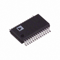
AD9051BRS Analog Devices Inc, AD9051BRS Datasheet - Page 10

AD9051BRS
Manufacturer Part Number
AD9051BRS
Description
IC ADC 10BIT 60MSPS 28-SSOP
Manufacturer
Analog Devices Inc
Specifications of AD9051BRS
Mounting Type
Surface Mount
Package / Case
28-SSOP (0.200", 5.30mm Width)
Rohs Status
RoHS non-compliant
Number Of Bits
10
Sampling Rate (per Second)
60M
Data Interface
Parallel
Number Of Converters
3
Power Dissipation (max)
315mW
Voltage Supply Source
Analog and Digital
Operating Temperature
-40°C ~ 85°C
Peak Reflow Compatible (260 C)
No
No. Of Bits
10 Bit
Leaded Process Compatible
No
No. Of Channels
2
Interface Type
Parallel
Number Of Elements
1
Resolution
10Bit
Architecture
Pipelined
Sample Rate
60MSPS
Input Polarity
Unipolar
Input Type
Voltage
Rated Input Volt
±0.625V
Differential Input
Yes
Power Supply Requirement
Single
Single Supply Voltage (typ)
5V
Dual Supply Voltage (typ)
Not RequiredV
Dual Supply Voltage (min)
Not RequiredV
Dual Supply Voltage (max)
Not RequiredV
Power Dissipation
315mW
Differential Linearity Error
1.5LSB
Integral Nonlinearity Error
1.5LSB
Operating Temp Range
-40C to 85C
Operating Temperature Classification
Industrial
Mounting
Surface Mount
Pin Count
28
Package Type
SSOP
Lead Free Status / Rohs Status
Not Compliant
Available stocks
Company
Part Number
Manufacturer
Quantity
Price
Company:
Part Number:
AD9051BRS-2V
Manufacturer:
AD
Quantity:
340
Part Number:
AD9051BRS-2V
Manufacturer:
ADI/亚德诺
Quantity:
20 000
Part Number:
AD9051BRSZ
Manufacturer:
ADI/亚德诺
Quantity:
20 000
Company:
Part Number:
AD9051BRSZ-2V
Manufacturer:
IML
Quantity:
3 000
Company:
Part Number:
AD9051BRSZRL
Manufacturer:
TOSHIBA
Quantity:
5 600
Part Number:
AD9051BRSZRL
Manufacturer:
ADI/亚德诺
Quantity:
20 000
AD9051
Overdrive of the Analog Input
Special care was taken in the design of the analog input section
of the AD9051 to prevent damage and corruption of data when
the input is overdriven. The nominal input range is 1.875 V to
3.125 V (1.25 V p-p centered at 2.5 V). Out-of-range compara-
tors detect when the analog input signal is out of this range and
the input buffer is clamped. The digital outputs are locked at
their maximum or minimum value (i.e., all “0” or all “1”). This
precludes the digital outputs changing to an invalid value when
the analog input is out of range.
The input is protected to one volt outside the power supply
rails. For nominal power (5 V and ground), the analog input
will not be damaged with signals from +5.5 V to –0.5 V.
Timing
The performance of the AD9051 is very insensitive to the duty
cycle of the clock. Pulsewidth variations of as much as ± 15% for
encode rates of 40 MSPS and ± 10% for encode rates of 60 MSPS
will cause no degradation in performance. (See Figure 17, SNR vs.
Duty Cycle.)
The AD9051 provides latched data outputs, with five pipeline
delays. Data outputs are available one propagation delay (t
after the rising edge of the encode command (refer to Figure 1,
Timing Diagram). The length of the output data lines and
loads placed on them should be minimized to reduce tran-
sients within the AD9051; these transients can detract from
the converter’s dynamic performance.
Power Dissipation
The power dissipation specification in the parameter table is
measured under the following conditions: encode is 60 MSPS,
analog input is –FS.
As shown in Figure 3, the actual power dissipation varies based
on these conditions. For instance, reducing the clock rate will
reduce power as expected for CMOS-type devices. The loading
determines the power dissipated in the output stages.
The analog input frequency and amplitude in conjunction with
the clock rate determine the switching rate of the output data
bits. Power dissipation increases as more data bits switch at
faster rates. For instance, if the input is a dc signal that is out of
range, no output bits will switch. This minimizes power in the
output stages, but is not realistic from a usage standpoint.
The dissipation in the output stages can be minimized by inter-
facing the outputs to 3 V logic (refer to Using the AD9051, 3 V
System). The lower output swings minimize power consumption
as follows: (1/2 C
Voltage Reference
A stable and accurate 2.5 V voltage reference is built into the
AD9051 (Pin 3, VREFOUT). In normal operation the internal
reference is used by strapping together Pins 3 and 4 of the
AD9051. The internal reference has 500 µA of extra drive cur-
rent that can be used for other circuits.
LOAD
× V
DD
2
× Update Rate).
PD
)
Some applications may require greater accuracy, improved
temperature performance, or adjustment of the gain of the
AD9051, which cannot be obtained by using the internal refer-
ence. For these applications, an external 2.5 V reference can be
used to connect to Pin 4 of the AD9051. The VREFIN requires
2 µA of drive current.
The input range can be adjusted by varying the reference
voltage applied to the AD9051. No appreciable degradation
in performance occurs when the reference is adjusted ± 5%.
The full-scale range of the ADC tracks reference voltage
changes linearly.
C


