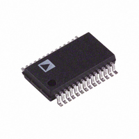
AD9051BRS Analog Devices Inc, AD9051BRS Datasheet - Page 5

AD9051BRS
Manufacturer Part Number
AD9051BRS
Description
IC ADC 10BIT 60MSPS 28-SSOP
Manufacturer
Analog Devices Inc
Specifications of AD9051BRS
Mounting Type
Surface Mount
Package / Case
28-SSOP (0.200", 5.30mm Width)
Rohs Status
RoHS non-compliant
Number Of Bits
10
Sampling Rate (per Second)
60M
Data Interface
Parallel
Number Of Converters
3
Power Dissipation (max)
315mW
Voltage Supply Source
Analog and Digital
Operating Temperature
-40°C ~ 85°C
Peak Reflow Compatible (260 C)
No
No. Of Bits
10 Bit
Leaded Process Compatible
No
No. Of Channels
2
Interface Type
Parallel
Number Of Elements
1
Resolution
10Bit
Architecture
Pipelined
Sample Rate
60MSPS
Input Polarity
Unipolar
Input Type
Voltage
Rated Input Volt
±0.625V
Differential Input
Yes
Power Supply Requirement
Single
Single Supply Voltage (typ)
5V
Dual Supply Voltage (typ)
Not RequiredV
Dual Supply Voltage (min)
Not RequiredV
Dual Supply Voltage (max)
Not RequiredV
Power Dissipation
315mW
Differential Linearity Error
1.5LSB
Integral Nonlinearity Error
1.5LSB
Operating Temp Range
-40C to 85C
Operating Temperature Classification
Industrial
Mounting
Surface Mount
Pin Count
28
Package Type
SSOP
Lead Free Status / Rohs Status
Not Compliant
Available stocks
Company
Part Number
Manufacturer
Quantity
Price
Company:
Part Number:
AD9051BRS-2V
Manufacturer:
AD
Quantity:
340
Part Number:
AD9051BRS-2V
Manufacturer:
ADI/亚德诺
Quantity:
20 000
Part Number:
AD9051BRSZ
Manufacturer:
ADI/亚德诺
Quantity:
20 000
Company:
Part Number:
AD9051BRSZ-2V
Manufacturer:
IML
Quantity:
3 000
Company:
Part Number:
AD9051BRSZRL
Manufacturer:
TOSHIBA
Quantity:
5 600
Part Number:
AD9051BRSZRL
Manufacturer:
ADI/亚德诺
Quantity:
20 000
Pin No.
1, 6, 7, 12, 21, 23
2, 8, 11
3
4
5
9
10
13
14
15
16–19
20, 22
24–27
28
C
VREFOUT
ENCODE
VREFIN
BWSEL
PIN CONFIGURATION
AINB
GND
GND
GND
GND
AIN
OR
V
V
V
D
D
D
10
11
12
13
14
1
2
3
4
5
6
7
8
9
Mnemonic
GND
V
VREFOUT
VREFIN
BWSEL
AINB
AIN
ENCODE
OR
D9 (MSB)
D8–D5
V
D4–D1
D0 (LSB)
D
DD
(Not to Scale)
TOP VIEW
AD9051
28
27
26
25
24
23
22
21
20
19
18
17
16
15
D0 (LSB)
D1
D2
D3
D4
GND
V
GND
V
D5
D6
D7
D8
D9 (MSB)
DD
DD
Description
Ground
Analog 5 V Power Supply
Internal Bandgap Voltage Reference (Nominally 2.5 V)
Input to Reference Amplifier. Voltage reference for ADC is connected here.
Bandwidth Select. NC = 130 MHz nominal. +V
Complementary Analog Input Pin (Analog Input Bar)
Analog Input Pin
Encode Clock Input to ADC. Internal T/H is placed in hold mode (ADC is encoding)
on rising edge of encode signal.
Out of Range Signal. Logic “0” when analog input is in nominal range. Logic “1” when
analog input is out of nominal range.
Most Significant Bit of ADC Output
Digital Output Bits of ADC
Digital Output Power Supply (Only Used by Digital Outputs)
Digital Output Bits of ADC
Least Significant Bit of ADC Output
PIN FUNCTION DESCRIPTIONS
AINB (PIN 9)
AIN (PIN 10)
OUTPUTS
ENCODE
DIGITAL
AIN
V
DD
+3V TO +5V
(PINS 20, 22)
N
t
EH
N – 5
t
A
t
t
EL
V
PD
D
N + 1
12k
12k
D0–D9, OR
D
N – 4
= 50 MHz nominal.
12k
12k
N + 2
INPUT
BUFFER
N – 3
N + 3
N – 2
ENCODE
(PIN 13)
N + 4
V
D
AD9051
N – 1
N + 5
VREF
(PIN 3)
N
V
D
OUT


