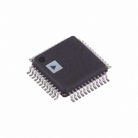
AD7661ASTZ Analog Devices Inc, AD7661ASTZ Datasheet - Page 23

AD7661ASTZ
Manufacturer Part Number
AD7661ASTZ
Description
IC ADC 16BIT W/REF 48-LQFP
Manufacturer
Analog Devices Inc
Series
PulSAR®r
Datasheet
1.AD7661ACPZRL.pdf
(28 pages)
Specifications of AD7661ASTZ
Data Interface
Serial, Parallel
Number Of Bits
16
Sampling Rate (per Second)
100k
Number Of Converters
1
Power Dissipation (max)
25mW
Voltage Supply Source
Analog and Digital
Operating Temperature
-40°C ~ 85°C
Mounting Type
Surface Mount
Package / Case
48-LQFP
Resolution (bits)
16bit
Input Channel Type
Pseudo Differential
Supply Voltage Range - Analogue
4.75V To 5.25V
Supply Voltage Range - Digital
2.7V To 5.25V,
Sampling Rate
100kSPS
Rohs Compliant
Yes
Number Of Elements
1
Resolution
16Bit
Architecture
SAR
Sample Rate
100KSPS
Input Polarity
Unipolar
Input Type
Voltage
Rated Input Volt
2.5V
Differential Input
Yes
Power Supply Requirement
Analog and Digital
Single Supply Voltage (typ)
5V
Single Supply Voltage (min)
4.75V
Single Supply Voltage (max)
5.25V
Dual Supply Voltage (typ)
Not RequiredV
Dual Supply Voltage (min)
Not RequiredV
Dual Supply Voltage (max)
Not RequiredV
Power Dissipation
45mW
Differential Linearity Error
-1LSB/1.5LSB
Integral Nonlinearity Error
±2.5LSB
Operating Temp Range
-40C to 85C
Operating Temperature Classification
Industrial
Mounting
Surface Mount
Pin Count
48
Package Type
LQFP
Input Signal Type
Pseudo-Differential
Lead Free Status / RoHS Status
Lead free / RoHS Compliant
For Use With
EVAL-AD7661CBZ - BOARD EVALUATION FOR AD7661
Lead Free Status / Rohs Status
Compliant
Available stocks
Company
Part Number
Manufacturer
Quantity
Price
Company:
Part Number:
AD7661ASTZ
Manufacturer:
ADI
Quantity:
390
Company:
Part Number:
AD7661ASTZ
Manufacturer:
Analog Devices Inc
Quantity:
10 000
Part Number:
AD7661ASTZ
Manufacturer:
ADI/亚德诺
Quantity:
20 000
Company:
Part Number:
AD7661ASTZRL
Manufacturer:
Analog Devices Inc
Quantity:
10 000
MASTER SERIAL INTERFACE
Internal Clock
The AD7661 is configured to generate and provide the serial
data clock SCLK when the EXT/ INT pin is held LOW. The
AD7661 also generates a SYNC signal to indicate to the host
when the serial data is valid. The serial clock SCLK and the
SYNC signal can be inverted if desired. Depending on the
RDC/SDIN input, the data can be read after each conversion or
during the following conversion. Figure 39 and Figure 40 show
detailed timing diagrams of these two modes.
CS, RD
CS, RD
CNVST
SDOUT
CNVST
SDOUT
BUSY
SYNC
SCLK
BUSY
SYNC
SCLK
t
16
t
3
Figure 40. Master Serial Data Timing for Reading (Read Previous Conversion during Convert)
t
t
t
14
15
16
t
t
t
14
15
29
t
17
X
t
t
18
22
Figure 39. Master Serial Data Timing for Reading (Read after Convert)
EXT/INT = 0
t
EXT/INT = 0
1
t
D15
3
t
X
t
1
20
22
t
19
t
21
t
20
D14
t
D15
2
23
1
t
19
t
18
Rev. 0 | Page 23 of 28
RDC/SDIN = 0
RDC/SDIN = 1
D14
t
21
2
t
3
23
t
28
3
Usually, because the AD7661 has a longer acquisition phase
than the conversion phase, the data is read immediately after
conversion. This makes the Master Read After Conversion the
most recommended serial mode when it can be used. In this
mode, it should be noted that unlike in other modes, the BUSY
signal returns LOW after the 16 data bits are pulsed out and not
at the end of the conversion phase, which results in a longer
BUSY width.
In the Read During Conversion mode, the serial clock and data
toggle at appropriate instants, which minimizes potential feed-
through between digital activity and critical conversion
decisions
INVSCLK = INVSYNC = 0
14
D2
INVSCLK = INVSYNC = 0
14
D2
15
D1
15
D1
16
t
24
16
t
30
D0
t
D0
24
t
t
t
t
t
t
25
26
27
25
26
27
AD7661


