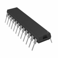
AD7856ANZ Analog Devices Inc, AD7856ANZ Datasheet - Page 5

AD7856ANZ
Manufacturer Part Number
AD7856ANZ
Description
IC ADC 14BIT 8CHAN 5V 24DIP
Manufacturer
Analog Devices Inc
Datasheet
1.AD7856ARSZ-REEL7.pdf
(32 pages)
Specifications of AD7856ANZ
Data Interface
8051, QSPI™, Serial, SPI™ µP
Number Of Bits
14
Sampling Rate (per Second)
285k
Number Of Converters
2
Power Dissipation (max)
89.25mW
Voltage Supply Source
Analog and Digital
Operating Temperature
-40°C ~ 105°C
Mounting Type
Through Hole
Package / Case
24-DIP (0.300", 7.62mm)
Resolution (bits)
14bit
Sampling Rate
285kSPS
Input Channel Type
Single Ended
Supply Voltage Range - Analog
4.75V To 5.25V
Supply Voltage Range - Digital
4.75V To 5.25V
Lead Free Status / RoHS Status
Lead free / RoHS Compliant
Available stocks
Company
Part Number
Manufacturer
Quantity
Price
Part Number:
AD7856ANZ
Manufacturer:
ADI/亚德诺
Quantity:
20 000
REV. A
TYPICAL TIMING DIAGRAMS
Figures 2 and 3 show typical read and write timing diagrams for
serial Interface Mode 2. The reading and writing occurs after
conversion in Figure 2, and during conversion in Figure 3. To
attain the maximum sample rate of 285 kHz, reading and writ-
ing must be performed during conversion as in Figure 3. At
least 330 ns acquisition time must be allowed (the time from
the falling edge of BUSY to the next rising edge of CONVST)
before the next conversion begins to ensure that the part is
settled to the 14-bit level. If the user does not want to provide
the CONVST signal, the conversion can be initiated in software
by writing to the control register.
Figure 3. Timing Diagram for Interface Mode 2 (Reading/Writing During Conversion)
Figure 2. Timing Diagram for Interface Mode 2 (Reading/Writing After Conversion)
CONVST (I/P)
DOUT (O/P)
CONVST (I/P)
BUSY (O/P)
DOUT (O/P)
SYNC (I/P)
BUSY (O/P)
SCLK (I/P)
SYNC (I/P)
SCLK (I/P)
DIN (I/P)
DIN (I/P)
t
2
t
2
t
1
t
1
THREE-STATE
t
THREE-STATE
CONVERT
t
t
1
1
t
= 100ns MIN,
t
4
t
= 100ns MIN,
t
4
CONVERT
CONVERT
t
3
t
3
DB15
DB15
t
7
t
= 3.5 s MAX, 5.25 s MAX FOR K VERSION
7
1
= 3.5 s MAX, 5.25 s MAX FOR K VERSION
1
DB15
t
–5–
t
DB15
4
4
t
= 30/50ns MAX A/K,
= 30/50ns MAX A/K,
t
6
6
t
8
t
t
8
CONVERT
Figure 1. Load Circuit for Digital Output Timing
Specifications
DB11
DB11
5
5
DB11
DB11
t
t
t
7
t
6
7
t
t
9
6
= 30/40ns MIN A/K
TO OUTPUT
= 30/40ns MIN A/K
9
t
6
t
10
6
10
PIN
DB0
DB0
100pF
16
16
C
DB0
L
t
DB0
11
t
11
200 A
1.6mA
t
t
12
12
THREE-
STATE
THREE-
STATE
I
I
OL
OL
+2.1V
AD7856


