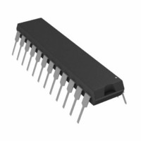
AD7731BNZ Analog Devices Inc, AD7731BNZ Datasheet - Page 11

AD7731BNZ
Manufacturer Part Number
AD7731BNZ
Description
IC ADC 24BIT SIGMA-DELTA 24DIP
Manufacturer
Analog Devices Inc
Datasheet
1.AD7731BRUZ.pdf
(44 pages)
Specifications of AD7731BNZ
Data Interface
DSP, Serial, SPI™
Number Of Bits
24
Sampling Rate (per Second)
6.4k
Number Of Converters
1
Power Dissipation (max)
125mW
Voltage Supply Source
Analog and Digital
Operating Temperature
-40°C ~ 85°C
Mounting Type
Through Hole
Package / Case
24-DIP (0.300", 7.62mm)
Resolution (bits)
24bit
Sampling Rate
6.4kSPS
Input Channel Type
Single Ended
Supply Voltage Range - Analog
4.75V To 5.25V
Supply Voltage Range - Digital
2.7V To 5.25V
Lead Free Status / RoHS Status
Lead free / RoHS Compliant
For Use With
EVAL-AD7731EBZ - BOARD EVALUATION FOR AD7731
Lead Free Status / RoHS Status
Lead free / RoHS Compliant, Lead free / RoHS Compliant
REV. A
Output Noise (CHP = 1, SKIP = 0)
Table III shows the output rms noise for some typical output update rates and –3 dB frequencies for the AD7731 when used in
chopping mode (CHP of Filter Register = 1) and with the second filter included in the loop. The numbers are generated with a mas-
ter clock frequency of 4.9152 MHz. These numbers are typical and generated at a differential analog input voltage of 0 V. The out-
put update rate is selected via the SF0 to SF11 bits of the Filter Register. Table IV, meanwhile, shows the output peak-to-peak
resolution in bits (rounded to the nearest 0.5 LSB) for the same output update rates. It is important to note that the numbers in
Table IV represent the resolution for which there will be no code flicker within a six-sigma limit. They are not calculated based on
rms noise but on peak-to-peak noise.
The numbers are generated for the bipolar input ranges. When the part is operated in unipolar mode, the output noise will be the
same as the equivalent bipolar input range. As a result, the numbers in Table III will remain the same for unipolar ranges. To calcu-
late the number for Table IV for unipolar input ranges simply subtract one from the peak-to-peak resolution number in bits.
Output
Data Rate Frequency Word
50 Hz
100 Hz
150 Hz
200 Hz
400 Hz
800 Hz
Output
Data Rate Frequency Word
50 Hz
100 Hz
150 Hz
200 Hz
400 Hz
800 Hz
ON-CHIP REGISTERS
The AD7731 contains 12 on-chip registers that can be accessed
via the serial port of the part. These registers are summarized in
Figure 4 and in Table V, and described in detail in the following
sections.
REV. 0
–3 dB
1.97 Hz
3.95 Hz
5.92 Hz
7.9 Hz
15.8 Hz
31.6 Hz
–3 dB
1.97 Hz
3.95 Hz
5.92 Hz
7.9 Hz
15.8 Hz
31.6 Hz
Table IV. Peak-to-Peak Resolution vs. Input Range and Update Rate (CHP = 1, SKIP = 0)
Table III. Output Noise vs. Input Range and Update Rate (CHP = 1, SKIP = 0)
SF
2048
1024
683
512
256
128
SF
2048
1024
683
512
256
128
Normal Fast Step
440 ms
220 ms
147 ms
110 ms
55 ms
27.5 ms
Normal Fast Step
440 ms
230 ms
147 ms
110 ms
55 ms
27.5 ms
Settling Time
Settling Time
40 ms
20 ms
13.3 ms
10 ms
5 ms
2.5 ms
40 ms
30 ms
13.3 ms
10 ms
5 ms
2.5 ms
Typical Output RMS Noise in nV
Peak-to-Peak Resolution in Bits
700
980
1230
1260
2000
3800
19
19
18.5
18.5
17.5
17
1.28 V
1.28 V
–11–
18.5
18
17.5
16.5
425
550
700
840
1230
2100
19
18
DIN
640 mV
640 mV
DOUT
DOUT
DOUT
DOUT
DOUT
DOUT
DOUT
DOUT
18.5
17.5
17
16
265
330
445
500
690
1400
18.5
18
320 mV
320 mV
Figure 4. Register Overview
DIN
DIN
DIN
DIN
DIN
DIN
Input Range
Input Range
170
270
430
760
18.5
18
17.5
17.5
17
16
COMMUNICATIONS REGISTER
230
340
160 mV
160 mV
OFFSET REGISTER (x3)
GAIN REGISTER (x3)
STATUS REGISTER
FILTER REGISTER
MODE REGISTER
DATA REGISTER
TEST REGISTER
RS2 RS1 RS0
120
190
210
245
335
590
18
17
17
17
16.5
15.5
80 mV
80 mV
85
115
140
170
215
345
17.5
17
16.5
16.5
16
15
40 mV
40 mV
AD7731
REGISTER
DECODER
SELECT
55
90
100
105
160
220
16
16
15.5
15
17
16
20 mV
20 mV


