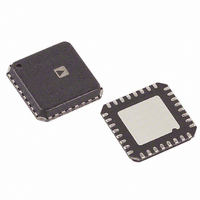
AD9237BCPZ-65 Analog Devices Inc, AD9237BCPZ-65 Datasheet - Page 6

AD9237BCPZ-65
Manufacturer Part Number
AD9237BCPZ-65
Description
IC ADC 12BIT SGL 65MSPS 32LFCSP
Manufacturer
Analog Devices Inc
Specifications of AD9237BCPZ-65
Data Interface
Parallel
Number Of Bits
12
Sampling Rate (per Second)
65M
Number Of Converters
3
Power Dissipation (max)
190mW
Voltage Supply Source
Single Supply
Operating Temperature
-40°C ~ 85°C
Mounting Type
Surface Mount
Package / Case
32-VFQFN, CSP Exposed Pad
Resolution (bits)
12bit
Input Channel Type
Differential
Supply Voltage Range - Analogue
2.7V To 3.6V
Supply Voltage Range - Digital
2.25V To 3.6V
Supply Current
64.5mA
Sampling Rate
65MSPS
Rohs Compliant
Yes
Number Of Elements
1
Resolution
12Bit
Architecture
Pipelined
Sample Rate
65MSPS
Input Polarity
Unipolar
Input Type
Voltage
Rated Input Volt
±0.5/±1/±2V
Differential Input
Yes
Power Supply Requirement
Single
Single Supply Voltage (typ)
3V
Single Supply Voltage (min)
2.7V
Single Supply Voltage (max)
3.6V
Dual Supply Voltage (typ)
Not RequiredV
Dual Supply Voltage (min)
Not RequiredV
Dual Supply Voltage (max)
Not RequiredV
Power Dissipation
270mW
Differential Linearity Error
±1.25LSB
Integral Nonlinearity Error
±2LSB
Operating Temp Range
-40C to 85C
Operating Temperature Classification
Industrial
Mounting
Surface Mount
Pin Count
32
Package Type
LFCSP EP
Lead Free Status / RoHS Status
Lead free / RoHS Compliant
Lead Free Status / RoHS Status
Lead free / RoHS Compliant, Lead free / RoHS Compliant
Available stocks
Company
Part Number
Manufacturer
Quantity
Price
Company:
Part Number:
AD9237BCPZ-65
Manufacturer:
CREE
Quantity:
101
AD9237
DEFINITIONS OF SPECIFICATIONS
INTEGRAL NONLINEARITY (INL)
INL refers to the deviation of each individual code from a line
drawn from “negative full scale” through “positive full scale.” The
point used as “negative full scale” occurs 1/2 LSB before the first
code transition. “Positive full scale” is defined as a level 1 1/2 LSB
beyond the last code transition. The deviation is measured from the
middle of each particular code to the true straight line.
DIFFERENTIAL NONLINEARITY (DNL, NO MISSING
CODES)
An ideal ADC exhibits code transitions that are exactly 1 LSB
apart. DNL is the deviation from this ideal value. Guaranteed no
missing codes to 12-bit resolution indicates that all 4096 codes,
respectively, must be present over all operating ranges.
ZERO ERROR
The major carry transition should occur for an analog value 1/2
LSB below VINA = VINB. Zero error is defined as the deviation
of the actual transition from that point.
GAIN ERROR
The first code transition should occur at an analog value 1/2 LSB
above negative full scale. The last transition should occur at an
analog value 1 1/2 LSB below the positive full scale. Gain error is
the deviation of the actual difference between first and last code
transitions and the ideal difference between first and last code
transitions.
TEMPERATURE DRIFT
The temperature drift for zero error and gain error specifies the
maximum change from the initial (25°C) value to the value at
TMIN or TMAX.
POWER SUPPLY REJECTION
The specification shows the maximum change in full scale from
the value with the supply at the minimum limit to the value with
the supply at its maximum limit.
APERTURE JITTER
Aperture jitter is the variation in aperture delay for successive
samples and can be manifested as noise on the input to the ADC.
APERTURE DELAY
Aperture delay is a measure of the sample-and-hold amplifier
(SHA) performance and is measured from the rising edge of the
clock input to when the input signal is held for conversion.
SIGNAL-TO-NOISE AND DISTORTION (S/N+D, SINAD)
RATIO
S/N+D is the ratio of the rms value of the measured input signal to
the rms sum of all other spectral components below the Nyquist
frequency, including harmonics but excluding dc. The value for
S/N+D is expressed in decibels.
AD9237 Preliminary Technical Information – 5/18/2005
–6–
EFFECTIVE NUMBER OF BITS (ENOB)
For a sine wave, SINAD can be expressed in terms of the number
of bits. Using the following formula,
it is possible to obtain a measure of performance expressed as N,
the effective number of bits.
Thus, effective number of bits for a device for sine wave inputs at
a given input frequency can be calculated directly from its
measured SINAD.
TOTAL HARMONIC DISTORTION (THD)
THD is the ratio of the rms sum of the first six harmonic
components to the rms value of the measured input signal and is
expressed as a percentage or in decibels.
SIGNAL-TO-NOISE RATIO (SNR)
SNR is the ratio of the rms value of the measured input signal to
the rms sum of all other spectral components below the Nyquist
frequency, excluding the first six harmonics and dc. The value for
SNR is expressed in decibels.
SPURIOUS FREE DYNAMIC RANGE (SFDR)
SFDR is the difference in dB between the rms amplitude of the
input signal and the peak spurious signal.
CLOCK PULSEWIDTH AND DUTY CYCLE
Pulsewidth high is the minimum amount of time that the clock
pulse should be left in the logic “1” state to achieve rated
performance: pulse width low is the minimum time the clock pulse
should be left in the low state. At a given clock rate, these specs
define an acceptable clock duty cycle.
MINIMUM CONVERSION RATE
The clock rate at which the SNR of the lowest analog signal
frequency drops by no more than 3 dB below the guaranteed limit.
MAXIMUM CONVERSION RATE
The clock rate at which parametric testing is performed.
OUTPUT PROPAGATION DELAY
The delay between the clock logic threshold and the time when all
bits are within valid logic levels.
TWO TONE SFDR
The ratio of the rms value of either input tone to the rms value of
the peak spurious component. The peak spurious component may
or may not be an IMD product. May be reported in dBc (i.e.,
degrades as signal levels are lowered) or in dBFS (always related
back to converter full scale).
Preliminary Technical Data
N = (SINAD – 1.76)/6.02
PrF


