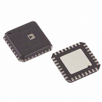
AD9237BCPZ-65 Analog Devices Inc, AD9237BCPZ-65 Datasheet - Page 7

AD9237BCPZ-65
Manufacturer Part Number
AD9237BCPZ-65
Description
IC ADC 12BIT SGL 65MSPS 32LFCSP
Manufacturer
Analog Devices Inc
Specifications of AD9237BCPZ-65
Data Interface
Parallel
Number Of Bits
12
Sampling Rate (per Second)
65M
Number Of Converters
3
Power Dissipation (max)
190mW
Voltage Supply Source
Single Supply
Operating Temperature
-40°C ~ 85°C
Mounting Type
Surface Mount
Package / Case
32-VFQFN, CSP Exposed Pad
Resolution (bits)
12bit
Input Channel Type
Differential
Supply Voltage Range - Analogue
2.7V To 3.6V
Supply Voltage Range - Digital
2.25V To 3.6V
Supply Current
64.5mA
Sampling Rate
65MSPS
Rohs Compliant
Yes
Number Of Elements
1
Resolution
12Bit
Architecture
Pipelined
Sample Rate
65MSPS
Input Polarity
Unipolar
Input Type
Voltage
Rated Input Volt
±0.5/±1/±2V
Differential Input
Yes
Power Supply Requirement
Single
Single Supply Voltage (typ)
3V
Single Supply Voltage (min)
2.7V
Single Supply Voltage (max)
3.6V
Dual Supply Voltage (typ)
Not RequiredV
Dual Supply Voltage (min)
Not RequiredV
Dual Supply Voltage (max)
Not RequiredV
Power Dissipation
270mW
Differential Linearity Error
±1.25LSB
Integral Nonlinearity Error
±2LSB
Operating Temp Range
-40C to 85C
Operating Temperature Classification
Industrial
Mounting
Surface Mount
Pin Count
32
Package Type
LFCSP EP
Lead Free Status / RoHS Status
Lead free / RoHS Compliant
Lead Free Status / RoHS Status
Lead free / RoHS Compliant, Lead free / RoHS Compliant
Available stocks
Company
Part Number
Manufacturer
Quantity
Price
Company:
Part Number:
AD9237BCPZ-65
Manufacturer:
CREE
Quantity:
101
Preliminary Technical Data
Pin No.
1
2
3
4
5,6
7-14, 17-20
15
16
21
22
23
24
25
26
27,32
28,31
29
30
AD9237 Preliminary Technical Information – 5/18/2005
Name
MODE 2
CLK
OE
PDWN
DNC
D0 (LSB) – D11 (MSB)
DGND
DRVDD
OTR
MODE
SENSE
VREF
REFB
REFT
AVDD
AGND
VIN+
VIN-
PIN FUNCTION DESCRIPTIONS (32 Pin LFCSP Package)
(LSB) D0
MODE 2
Preliminary LFCSP Pin Configuration
PDW N
CLK
O E
NC
NC
D1
1
2
3
4
5
6
7
8
Function
SHA Gain Select and Power Control (see Figure 2)
Clock Input Pin
Output Enable Pin (active low)
Power-Down function selection.
Do Not Connect
Data Output Pins
Digital ground.
Digital Output Driver Supply.
Out of Range Flag
Output Data Format Select and Duty Cycle Stabilizer Control
Reference mode/Input Full Scale Select
Voltage Reference Input/Output.
Differential Reference (-).
Differential Reference (+).
Analog Power Supply.
Analog ground.
Analog Input Pin (+).
Analog Input Pin (-).
MODE2 Connection
AVDD
2/3 AVDD
1/3 AVDD
AGND
PWDN
AVDD
1/3 AVDD
AGND
MODE Connection
AVDD
2/3 AVDD
1/3 AVDD
AGND
Chip Scale Package
(Not to Scale)
AD9237BCP
–7–
Lead Fram e
Top View
Function
Power Down Mode: All circuits powered down, no clock
Standby Mode: Only current & voltage references powered up
Power Up
Output Data Format
Twos Complement
Twos Complement
Offset Binary
Offset Binary
SHA Gain
24
23
22
21
20
19
18
17
1
1
2
2
VREF
SENSE
MODE
OTR
D11 (MSB)
D10
D9
D8
Duty Cycle Stabilizer
Auto Power Control
AD9237
Disabled
Disabled
Disabled
Disabled
Enabled
Enabled
Enabled
Enabled
REV
PrF


