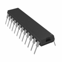
AD7710ANZ Analog Devices Inc, AD7710ANZ Datasheet - Page 3

AD7710ANZ
Manufacturer Part Number
AD7710ANZ
Description
IC ADC SIGNAL CONDITIONING 24DIP
Manufacturer
Analog Devices Inc
Datasheet
1.AD7710ARZ-REEL.pdf
(32 pages)
Specifications of AD7710ANZ
Data Interface
Serial
Number Of Bits
24
Sampling Rate (per Second)
1.03k
Number Of Converters
1
Power Dissipation (max)
45mW
Voltage Supply Source
Analog and Digital, Dual ±
Operating Temperature
-40°C ~ 85°C
Mounting Type
Through Hole
Package / Case
24-DIP (0.300", 7.62mm)
Resolution (bits)
24bit
Sampling Rate
1.02kSPS
Input Channel Type
Single Ended
Supply Voltage Range - Digital
4.75V To 5.25V
Supply Current
4.5mA
Digital Ic Case Style
DIP
Lead Free Status / RoHS Status
Lead free / RoHS Compliant
Available stocks
Company
Part Number
Manufacturer
Quantity
Price
Part Number:
AD7710ANZ
Manufacturer:
ADI/亚德诺
Quantity:
20 000
Parameter
REFERENCE OUTPUT
V
LOGIC INPUTS
LOGIC OUTPUTS
TRANSDUCER BURNOUT
COMPENSATION CURRENT
SYSTEM CALIBRATION
NOTES
12
13
14
15
REV. G
The AD7710 is tested with the following V
Guaranteed by design, not production tested.
After calibration, if the analog input exceeds positive full scale, the converter will output all 1s. If the analog input is less than negative full scale then the device will
These calibration and span limits apply, provided the absolute voltage on the analog inputs does not exceed AV
BIAS
AV
output all 0s.
The offset calibration limit applies to both the unipolar zero point and the bipolar zero point.
Output Voltage
Initial Tolerance @ 25 C
Drift
Output Noise
Line Regulation (AV
Load Regulation
External Current
Input Voltage Range
V
Input Current
All Inputs Except MCLK IN
MCLK IN Only
V
V
Floating State Leakage Current
Floating State Output Capacitance
Current
Initial Tolerance @ 25 C
Drift
Output Current
Initial Tolerance @ 25 C
Drift
Line Regulation (AV
Load Regulation
Output Compliance
Positive Full-Scale Calibration Limit
Negative Full-Scale Calibration Limit
Offset Calibration Limits
Input Span
BIAS
OL
OH
DD
V
V
V
V
INPUT
, Output Low Voltage
INL
INH
INL
INH
, Output High Voltage
= 5 V and V
Rejection
, Input Low Voltage
, Input Low Voltage
, Input High Voltage
, Input High Voltage
15
12
SS
= –5 V, V
DD
DD
)
)
15
BIAS
= 0 V.
13
BIAS
l4
l4
voltages. With AV
A, S Versions
2.5
20
30
1
1.5
1
AV
or AV
or AV
V
or V
or V
65 to 85
0.8
2.0
0.8
3.5
0.4
DV
9
4.5
0.1
20
35
20
20
AV
(1.05
–(1.05
–(1.05
0.8
(2.1
1
10
10
10
4
SS
DD
DD
DD
+ 0.85
SS
SS
V
DD
DD
– 0.85
– 2
– 1
V
+ 3
+ 2.1
REF
V
REF
V
V
– 3.5
– 2.1
REF
/GAIN
REF
REF
DD
)/GAIN
)/GAIN
V
)/GAIN
)/GAIN
= 5 V and V
1
REF
V
REF
–3–
Unit
V nom
% max
ppm/ C typ
mV/V max
mV/mA max Maximum Load Current 1 mA
mA max
V max
V max
V min
V min
dB typ
V max
V min
V max
V min
V max
V min
pF typ
% typ
%/ C typ
ppm/ C typ
nA/V max
nA/V max
V max
V max
V max
V max
V min
V max
SS
V typ
A max
A nom
A max
A nom
= 0 V, V
max
BIAS
= 2.5 V; with AV
Conditions/Comments
Peak-peak Noise 0.1 Hz to 10 Hz Bandwidth
See V
Whichever Is Smaller: +5 V/–5 V or +10 V/0 V
Nominal AV
Whichever Is Smaller; +5 V/0 V Nominal AV
See V
Whichever Is Greater; +5 V/–5 V or +10 V/0 V
Nominal AV
Whichever Is Greater; +5 V/0 V Nominal AV
Increasing with Gain
I
I
AV
GAIN Is the Selected PGA Gain (Between 1 and 128)
GAIN Is the Selected PGA Gain (Between 1 and 128)
GAIN Is the Selected PGA Gain (Between 1 and 128)
GAIN Is the Selected PGA Gain (Between 1 and 128)
GAIN Is the Selected PGA Gain (Between 1 and 128)
SINK
SOURCE
DD
= 1.6 mA
BIAS
BIAS
= +5 V
= 100 A
Input Section
Input Section
DD
DD
DD
DD
+ 30 mV or go more negative than V
/V
/V
= 10 V and V
SS
SS
SS
= 0 V, V
BIAS
= 5 V; and with
AD7710
SS
DD
DD
– 30 mV.
/V
/V
SS
SS


