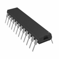
AD7710ANZ Analog Devices Inc, AD7710ANZ Datasheet - Page 8

AD7710ANZ
Manufacturer Part Number
AD7710ANZ
Description
IC ADC SIGNAL CONDITIONING 24DIP
Manufacturer
Analog Devices Inc
Datasheet
1.AD7710ARZ-REEL.pdf
(32 pages)
Specifications of AD7710ANZ
Data Interface
Serial
Number Of Bits
24
Sampling Rate (per Second)
1.03k
Number Of Converters
1
Power Dissipation (max)
45mW
Voltage Supply Source
Analog and Digital, Dual ±
Operating Temperature
-40°C ~ 85°C
Mounting Type
Through Hole
Package / Case
24-DIP (0.300", 7.62mm)
Resolution (bits)
24bit
Sampling Rate
1.02kSPS
Input Channel Type
Single Ended
Supply Voltage Range - Digital
4.75V To 5.25V
Supply Current
4.5mA
Digital Ic Case Style
DIP
Lead Free Status / RoHS Status
Lead free / RoHS Compliant
Available stocks
Company
Part Number
Manufacturer
Quantity
Price
Part Number:
AD7710ANZ
Manufacturer:
ADI/亚德诺
Quantity:
20 000
AD7710
Pin
19
20
21
22
23
24
Terminology Integral Nonlinearity
This is the maximum deviation of any code from a straight line
passing through the endpoints of the transfer function. The
endpoints of the transfer function are zero scale (not to be con-
fused with bipolar zero), a point 0.5 LSB below the first code
transition (000 . . . 000 to 000 . . . 001) and full scale, a point
0.5 LSB above the last code transition (111 . . . 110 to 111 . . .
111). The error is expressed as a percentage of full scale.
Positive Full-Scale Error
Positive full-scale error is the deviation of the last code transi-
tion (111 . . . 110 to 111 . . . 111) from the ideal AIN(+) voltage
(AIN(–) + V
and bipolar analog input ranges.
Unipolar Offset Error
Unipolar offset error is the deviation of the first code transition
from the ideal AIN(+) voltage (AIN(–) + 0.5 LSB) when oper-
ating in the unipolar mode.
Bipolar Zero Error
This is the deviation of the midscale transition (0111 . . . 111 to
1000 . . . 000) from the ideal AIN(+) voltage (AIN(–) – 0.5 LSB)
when operating in the bipolar mode.
Bipolar Negative Full-Scale Error
This is the deviation of the first code transition from the ideal
AIN(+) voltage (AIN(–) – V
ing in the bipolar mode.
Mnemonic
TFS
RFS
DRDY
SDATA
DGND
DV
DD
REF
/GAIN – 3/2 LSBs). It applies to both unipolar
Serial Data. Input/output with serial data being written to either the control register or the calibration regis-
Ground Reference Point for Digital Circuitry.
Function
Transmit Frame Synchronization. Active low logic input used to write serial data to the device with serial data
expected after the falling edge of this pulse. In the self-clocking mode, the serial clock becomes active after
TFS goes low. In the external clocking mode, TFS must go low before the first bit of the data-word is written
to the part.
Receive Frame Synchronization. Active low logic input used to access serial data from the device. In the
self-clocking mode, the SCLK and SDATA lines both become active after RFS goes low. In the external
clocking mode, the SDATA line becomes active after RFS goes low.
Logic Output. A falling edge indicates that a new output word is available for transmission. The DRDY pin
will return high upon completion of transmission of a full output word. DRDY is also used to indicate when
the AD7710 has completed its on-chip calibration sequence.
ters, and serial data being accessed from the control register, calibration registers, or the data register.
During an output data read operation, serial data becomes active after RFS goes low (provided DRDY is low).
During a write operation, valid serial data is expected on the rising edges of SCLK when TFS is low. The
output data coding is natural binary for unipolar inputs and offset binary for bipolar inputs.
Digital Supply Voltage, 5 V. DV
REF
/GAIN + 0.5 LSB) when operat-
DD
should not exceed AV
–8–
Positive Full-Scale Overrange
Positive full-scale overrange is the amount of overhead available
to handle input voltages on AIN(+) input greater than AIN(–) +
V
system gain errors in system calibration routines) without intro-
ducing errors due to overloading the analog modulator or to
overflowing the digital filter.
Negative Full-Scale Overrange
This is the amount of overhead available to handle voltages on
AIN(+) below AIN(–) –V
analog modulator or overflowing the digital filter. Note that the
analog input will accept negative voltage peaks even in the uni-
polar mode provided that AIN(+) is greater than AIN(–) and
greater than V
Offset Calibration Range
In the system calibration modes, the AD7710 calibrates its offset
with respect to the analog input. The offset calibration range
specification defines the range of voltages that the AD7710 can
accept and still calibrate offset accurately.
Full-Scale Calibration Range
This is the range of voltages that the AD7710 can accept in the
system calibration mode and still calibrate full scale correctly.
Input Span
In system calibration schemes, two voltages applied in sequence
to the AD7710’s analog input define the analog input range.
The input span specification defines the minimum and maxi-
mum input voltages from zero- to full-scale that the AD7710 can
accept and still calibrate gain accurately.
REF
/GAIN (for example, noise peaks or excess voltages due to
DD
SS
by more than 0.3 V in normal operation.
– 30 mV.
REF
/GAIN without overloading the
REV. G


