AD9240AS Analog Devices Inc, AD9240AS Datasheet - Page 4
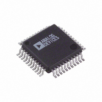
AD9240AS
Manufacturer Part Number
AD9240AS
Description
IC ADC 14BIT 10MSPS 44-MQFP
Manufacturer
Analog Devices Inc
Datasheet
1.AD9240ASZ.pdf
(24 pages)
Specifications of AD9240AS
Mounting Type
Surface Mount
Rohs Status
RoHS non-compliant
Number Of Bits
14
Sampling Rate (per Second)
10M
Data Interface
Parallel
Number Of Converters
7
Power Dissipation (max)
330mW
Voltage Supply Source
Analog and Digital
Operating Temperature
-40°C ~ 85°C
Package / Case
44-MQFP, 44-PQFP
Power Dissipation Pd
330mW
Input Channels Per Adc
2
No. Of Channels
2
Peak Reflow Compatible (260 C)
No
Sample Rate
10MSPS
Supply Voltage Max
5V
No. Of Bits
14 Bit
For Use With
AD9240-EB - BOARD EVAL FOR AD9240
Lead Free Status / RoHS Status
Contains lead / RoHS non-compliant
Available stocks
Company
Part Number
Manufacturer
Quantity
Price
Company:

Part Number:
AD9240AS
Manufacturer:
AD
Quantity:
5 510
Part Number:
AD9240AS
Manufacturer:
ADI/亚德诺
Quantity:
20 000
Company:
Part Number:
AD9240ASRL
Manufacturer:
Analog Devices Inc
Quantity:
10 000
Company:
Part Number:
AD9240ASZ
Manufacturer:
ADI
Quantity:
850
Company:
Part Number:
AD9240ASZ
Manufacturer:
Analog Devices Inc
Quantity:
10 000
Part Number:
AD9240ASZ
Manufacturer:
ADI/亚德诺
Quantity:
20 000
Company:
Part Number:
AD9240ASZRL
Manufacturer:
MAXIM
Quantity:
495


CAUTION
ESD (electrostatic discharge) sensitive device. Electrostatic charges as high as 4000 V readily
accumulate on the human body and test equipment and can discharge without detection.
Although the AD9240 features proprietary ESD protection circuitry, permanent damage may
occur on devices subjected to high energy electrostatic discharges. Therefore, proper ESD
precautions are recommended to avoid performance degradation or loss of functionality.
AD9240
ABSOLUTE MAXIMUM RATINGS*
Parameter
AVDD
DVDD
AVSS
AVDD
DRVDD
DRVSS
REFCOM
CLK
Digital Outputs
VINA, VINB
VREF
SENSE
CAPB, CAPT
BIAS
Junction Temperature
Storage Temperature
Lead Temperature
*Stresses above those listed under Absolute Maximum Ratings may cause perma-
SWITCHING SPECIFICATIONS
Parameters
Clock Period
CLOCK Pulsewidth High
CLOCK Pulsewidth Low
Output Delay
Pipeline Delay (Latency)
NOTES
1
Specifications subject to change without notice.
The clock period may be extended to 1 ms without degradation in specified performance @ +25 C.
nent damage to the device. This is a stress rating only; functional operation of the
device at these or any other conditions above those indicated in the operational
sections of this specification is not implied. Exposure to absolute maximum ratings
for extended periods may effect device reliability.
ANALOG
(10 sec)
OUTPUT
CLOCK
INPUT
INPUT
DATA
1
S1
t
CH
Figure 1. Timing Diagram
t
C
t
CL
With
Respect
to
AVSS
DVSS
DVSS
DVDD
DRVSS
AVSS
AVSS
AVSS
AVSS
AVSS
AVSS
DRVSS
AVSS
AVSS
S2
Min
–0.3
–0.3
–0.3
–6.5
–0.3
–0.3
–0.3
–0.3
–0.3
–0.3
–0.3
–0.3
–0.3
–0.3
–65
S3
Max
+6.5
+6.5
+0.3
+6.5
+6.5
+0.3
+0.3
AVDD + 0.3
DRVDD + 0.3 V
AVDD + 0.3
AVDD + 0.3
AVDD + 0.3
AVDD + 0.3
AVDD + 0.3
+150
+150
+300
(T
MIN
Symbol
t
t
t
t
C
CH
CL
OD
S4
to T
t
OD
MAX
DATA 1
with AVDD = +5 V, DVDD = +5 V, DRVDD = +5 V, R
Units
V
V
V
V
V
V
V
V
V
V
V
V
V
C
C
C
–4–
THERMAL CHARACTERISTICS
Thermal Resistance
44-Lead MQFP
(LSB) BIT 14
NC = NO CONNECT
JA
JC
= 53.2 C/W
= 19 C/W
DRVDD
DRVSS
DVSS
AVSS
DVDD
AVDD
CLK
NC
NC
NC
10
11
1
2
3
4
5
6
7
8
9
100
45
45
8
13
19
3
AD9240
44
12 13 14 15 16 17 18 19 20 21 22
PIN 1
IDENTIFIER
PIN CONFIGURATION
43
42
41
(Not to Scale)
AD9240
TOP VIEW
40 39 38
WARNING!
BIAS
37
= 2 k , C
36 35 34
ESD SENSITIVE DEVICE
L
Units
ns min
ns min
ns min
ns min
ns typ
ns max
Clock Cycles
= 20 pF)
32
31
30
29
28
27
26
25
24
23
33
REFCOM
SENSE
NC
AVSS
AVDD
NC
NC
OTR
BIT 1 (MSB)
BIT 2
VREF
REV.
B
Related parts for AD9240AS
Image
Part Number
Description
Manufacturer
Datasheet
Request
R

Part Number:
Description:
BOARD EVAL FOR AD9240
Manufacturer:
Analog Devices Inc
Datasheet:

Part Number:
Description:
±1.7g Dual-Axis IMEMS Accelerometer Evaluation Board
Manufacturer:
Analog Devices Inc
Datasheet:
Part Number:
Description:
Inertial Sensor Evaluation System
Manufacturer:
Analog Devices Inc
Datasheet:
Part Number:
Description:
Manufacturer:
Analog Devices Inc
Datasheet:
Part Number:
Description:
Manufacturer:
Analog Devices Inc
Datasheet:
Part Number:
Description:
Manufacturer:
Analog Devices Inc
Datasheet:
Part Number:
Description:
Manufacturer:
Analog Devices Inc
Datasheet:
Part Number:
Description:
Manufacturer:
Analog Devices Inc
Datasheet:
Part Number:
Description:
Manufacturer:
Analog Devices Inc
Datasheet:
Part Number:
Description:
Manufacturer:
Analog Devices Inc
Datasheet:
Part Number:
Description:
Manufacturer:
Analog Devices Inc
Datasheet:
Part Number:
Description:
Manufacturer:
Analog Devices Inc
Datasheet:
Part Number:
Description:
Manufacturer:
Analog Devices Inc
Datasheet: