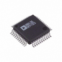
AD9240AS Analog Devices Inc, AD9240AS Datasheet - Page 9

AD9240AS
Manufacturer Part Number
AD9240AS
Description
IC ADC 14BIT 10MSPS 44-MQFP
Manufacturer
Analog Devices Inc
Datasheet
1.AD9240ASZ.pdf
(24 pages)
Specifications of AD9240AS
Mounting Type
Surface Mount
Rohs Status
RoHS non-compliant
Number Of Bits
14
Sampling Rate (per Second)
10M
Data Interface
Parallel
Number Of Converters
7
Power Dissipation (max)
330mW
Voltage Supply Source
Analog and Digital
Operating Temperature
-40°C ~ 85°C
Package / Case
44-MQFP, 44-PQFP
Power Dissipation Pd
330mW
Input Channels Per Adc
2
No. Of Channels
2
Peak Reflow Compatible (260 C)
No
Sample Rate
10MSPS
Supply Voltage Max
5V
No. Of Bits
14 Bit
For Use With
AD9240-EB - BOARD EVAL FOR AD9240
Lead Free Status / RoHS Status
Contains lead / RoHS non-compliant
Available stocks
Company
Part Number
Manufacturer
Quantity
Price
Company:
Part Number:
AD9240AS
Manufacturer:
AD
Quantity:
5 510
Part Number:
AD9240AS
Manufacturer:
ADI/亚德诺
Quantity:
20 000
Company:
Part Number:
AD9240ASRL
Manufacturer:
Analog Devices Inc
Quantity:
10 000
Company:
Part Number:
AD9240ASZ
Manufacturer:
ADI
Quantity:
850
Company:
Part Number:
AD9240ASZ
Manufacturer:
Analog Devices Inc
Quantity:
10 000
Part Number:
AD9240ASZ
Manufacturer:
ADI/亚德诺
Quantity:
20 000
Company:
Part Number:
AD9240ASZRL
Manufacturer:
MAXIM
Quantity:
495
The addition of a differential input structure gives the user an
additional level of flexibility that is not possible with traditional
flash converters. The input stage allows the user to easily con-
figure the inputs for either single-ended operation or differential
operation. The A/D’s input structure allows the dc offset of the
input signal to be varied independently of the input span of the
converter. Specifically, the input to the A/D core is the differ-
ence of the voltages applied at the VINA and VINB input pins.
Therefore, the equation,
defines the output of the differential input stage and provides
the input to the A/D core.
The voltage, V
(2)
where VREF is the voltage at the VREF pin.
While an infinite combination of VINA and VINB inputs exist
that satisfy Equation 2, there is an additional limitation placed
on the inputs by the power supply voltages of the AD9240. The
power supplies bound the valid operating range for VINA and
VINB. The condition,
(3)
where AVSS is nominally 0 V and AVDD is nominally +5 V,
defines this requirement. Thus, the range of valid inputs for
VINA and VINB is any combination that satisfies both Equa-
tions 2 and 3.
For additional information showing the relationship between
VINA, VINB, VREF and the digital output of the AD9240, see
Table IV.
Refer to Table I and Table II for a summary of the various
analog input and reference configurations.
ANALOG INPUT OPERATION
Figure 24 shows the equivalent analog input of the AD9240
which consists of a differential sample-and-hold amplifier (SHA).
The differential input structure of the SHA is highly flexible,
allowing the devices to be easily configured for either a differen-
tial or single-ended input. The dc offset, or common-mode
voltage, of the input(s) can be set to accommodate either single-
supply or dual supply systems. Note also that the analog inputs,
VINA and VINB, are interchangeable with the exception that
reversing the inputs to the VINA and VINB pins results in a
polarity inversion.
REV.
B
VINB
VINA
Figure 24. Simplified Input Circuit
CORE
AVSS – 0.3 V < VINA < AVDD + 0.3 V
AVSS – 0.3 V < VINB < AVDD + 0.3 V
, must satisfy the condition,
V
–VREF
C
C
C
C
PIN
PAR
PIN
PAR
CORE
+
–
= VINA – VINB
Q
Q
S1
S1
V
CORE
Q
H1
C
C
VREF
S
S
C
C
H
H
Q
Q
S2
S2
(1)
–9–
The input SHA of the AD9240 is optimized to meet the perfor-
mance requirements for some of the most demanding commu-
nication, imaging, and data acquisition applications while
maintaining low power dissipation. Figure 25 is a graph of the
full-power bandwidth of the AD9240, typically 60 MHz. Note
that the small signal bandwidth is the same as the full-power
bandwidth. The settling time response to a full-scale stepped
input is shown in Figure 26 and is typically less than 40 ns to
0.0025%. The low input referred noise of 0.36 LSB’s rms is
displayed via a grounded histogram and is shown in Figure 13.
The SHA’s optimum distortion performance for a differential or
single-ended input is achieved under the following two condi-
tions: (1) the common-mode voltage is centered around mid-
supply (i.e., AVDD/2 or approximately 2.5 V) and (2) the input
signal voltage span of the SHA is set at its lowest (i.e., 2 V input
span). This is due to the sampling switches, Q
switches whose R
dependency which causes frequency dependent ac distortion
while the SHA is in the track mode. The R
CMOS switch is typically lowest at its midsupply but increases
symmetrically as the input signal approaches either AVDD or
AVSS. A lower input signal voltage span centered at midsupply
reduces the degree of R
16000
12000
–10
8000
4000
–1
–2
–3
–4
–5
–6
–7
–8
–9
1
0
1
0
0
Figure 25. Full-Power Bandwidth
10
ON
Figure 26. Settling Time
resistance is very low but has some signal
20
ON
FREQUENCY – MHz
modulation.
SETTLING TIME – ns
30
10
40
50
ON
60
resistance of a
S1
AD9240
, being CMOS
70
100
80


