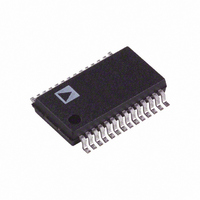
AD9226ARSZ Analog Devices Inc, AD9226ARSZ Datasheet - Page 21

AD9226ARSZ
Manufacturer Part Number
AD9226ARSZ
Description
IC ADC 12BIT 65MSPS 28-SSOP
Manufacturer
Analog Devices Inc
Datasheet
1.AD9226ASTZ.pdf
(28 pages)
Specifications of AD9226ARSZ
Data Interface
Parallel
Number Of Bits
12
Sampling Rate (per Second)
65M
Number Of Converters
3
Power Dissipation (max)
475mW
Voltage Supply Source
Single Supply
Operating Temperature
-40°C ~ 85°C
Mounting Type
Surface Mount
Package / Case
28-SSOP (0.200", 5.30mm Width)
Resolution (bits)
12bit
Sampling Rate
65MSPS
Input Channel Type
Differential, Single Ended
Supply Voltage Range - Analog
4.75V To 5.25V
Supply Current
86mA
Lead Free Status / RoHS Status
Lead free / RoHS Compliant
For Use With
AD9226-EB - BOARD EVAL FOR AD9226-SSOP
Lead Free Status / RoHS Status
Lead free / RoHS Compliant, Lead free / RoHS Compliant
Available stocks
Company
Part Number
Manufacturer
Quantity
Price
Part Number:
AD9226ARSZ
Manufacturer:
ADI/亚德诺
Quantity:
20 000
Part Number:
AD9226ARSZRL
Manufacturer:
ADI/亚德诺
Quantity:
20 000
VR
VR is an internal bias point on the LQFP package. It must be
decoupled to ground with a 0.1 µF capacitor.
The digital activity on the AD9226 chip falls into two general
categories: correction logic and output drivers. The internal
correction logic draws relatively small surges of current, mainly
during the clock transitions. The output drivers draw large
current impulses while the output bits are changing. The size
and duration of these currents are a function of the load on the
output bits: large capacitive loads are to be avoided.
For the digital decoupling shown in Figure 19, 0.1 µF ceramic
chip and 10 µF tantalum capacitors are appropriate. Reason-
able capacitive loads on the data pins are less than 20 pF per
bit. Applications involving greater digital loads should consider
increasing the digital decoupling proportionally and/or using
external buffers/latches.
A complete decoupling scheme will also include large tantalum
or electrolytic capacitors on the power supply connector to
reduce low-frequency ripple to negligible levels.
EVALUATION BOARD AND TYPICAL BENCH
CHARACTERIZATION TEST SETUP
The AD9226 evaluation board is configured to operate upon
applying both power and the analog and clock input signals. It
provides three possible analog input interfaces to characterize
the AD9226’s ac and dc performance. For ac characterization, it
provides a transformer coupled input with the common-mode
input voltage (CMV) set to AVDD/2. Note, the evaluation
board is shipped with a transformer coupled interface and a 2 V
input span. For differential dc coupled applications, the evalua-
tion board has provisions to be driven by the AD8138 amplifier.
If a single-ended input is desired, it may be driven through the
S3 connector. The various input signal options are accessible by
the jumper connections. Refer to the Evaluation Board schematic.
REFIN
10MHz
REFOUT
SIGNAL SYNTHESIZER
65(OR 260MHz), 4V p-p
65(OR 260MHz), 4V p-p
CLK SYNTHESIZER
HP8644
HP8644
BANDPASS FILTER
1MHz
AVDD
S4
INPUT
xFMR
S1
INPUT
CLOCK
The clock input signal to the AD9226 evaluation board can be
applied to one of two inputs, CLOCK and AUXCLK. The
CLOCK input should be selected if the frequency of the input
clock signal is at the target sample rate of the AD9226. The
input clock signal is ac-coupled and level-shifted to the switch-
ing threshold of a 74VHC02 clock driver. The AUXCLK input
should be selected in applications requiring the lowest jitter and
SNR performance (i.e., IF Undersampling characterization). It
allows the user to apply a clock input signal that is 4× the target
sample rate of the AD9226. A low-jitter, differential divide-by-4
counter, the MC100EL33D, provides a 1× clock output that is
subsequently returned back to the CLOCK input via JP7. For
example, a 260 MHz signal (sinusoid) will be divided down to
a 65 MHz signal for clocking the ADC. Note, R1 must be
removed with the AUXCLK interface. Lower jitter is often
achieved with this interface since many RF signal generators
display improved phase noise at higher output frequencies and
the slew rate of the sinusoidal output signal is 4× that of a 1×
signal of equal amplitude.
Figure 20 shows the bench characterization setup used to evalu-
ate the AD9226’s ac performance for many of the data sheet
characterization curves. Signal and Clock RF generators A and
B are high-frequency, “very” low-phase noise frequency sources.
These generators should be phase locked by sharing the same
10 MHz REF signal (located on the instruments back panel) to
allow for nonwindowed, coherent FFTs. Also, the AUXCLK
option on the AD9226 evaluation board should be used to
achieve the best SNR performance. Since the distortion and
broadband noise of an RF generator can often be a limiting
factor in measuring the true performance of an ADC, a high Q
passive bandpass filter should be inserted between the generator
and AD9226 evaluation board.
5V
EVALUATION BOARD
GND
5V
AUX CLOCK
AVDD
AD9226
DUT
( 4)
S4
GND
3V
DVDD
DUT
OUTPUT
WORD
DVDD
3V
(P1)
EQUIPMENT
DSP
AD9226


