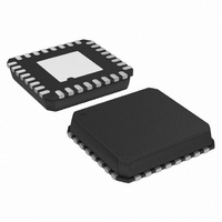
AD7626BCPZ Analog Devices Inc, AD7626BCPZ Datasheet - Page 22

AD7626BCPZ
Manufacturer Part Number
AD7626BCPZ
Description
IC ADC 16BIT 10MSPS DIFF 32LFCSP
Manufacturer
Analog Devices Inc
Datasheet
1.AD7626BCPZ-RL7.pdf
(28 pages)
Specifications of AD7626BCPZ
Data Interface
Serial
Design Resources
Single-Ended-to-Differential High Speed Drive Circuit for 16-Bit, 10 MSPS AD7626 ADC (CN0105)
Number Of Bits
16
Sampling Rate (per Second)
10M
Number Of Converters
1
Power Dissipation (max)
170mW
Voltage Supply Source
Single Supply
Operating Temperature
-40°C ~ 85°C
Mounting Type
Surface Mount
Package / Case
32-VFQFN, CSP Exposed Pad
Resolution (bits)
16bit
Sampling Rate
10MSPS
Input Channel Type
Differential
Supply Current
23.5mA
Digital Ic Case Style
CSP
No. Of Pins
32
Lead Free Status / RoHS Status
Lead free / RoHS Compliant
Available stocks
Company
Part Number
Manufacturer
Quantity
Price
Company:
Part Number:
AD7626BCPZ
Manufacturer:
ADI
Quantity:
263
Part Number:
AD7626BCPZ
Manufacturer:
ADI/亚德诺
Quantity:
20 000
Company:
Part Number:
AD7626BCPZ-RL7
Manufacturer:
PERICOM
Quantity:
101
Part Number:
AD7626BCPZ-RL7
Manufacturer:
ADI/亚德诺
Quantity:
20 000
AD7626
DIGITAL INTERFACE
Conversion Control
All analog-to-digital conversions are controlled by the CNV±
signal. This signal can be applied in the form of a CNV+/CNV−
LVDS signal, or it can be applied in the form of a 2.5 V CMOS
logic signal to the CNV+ pin. The conversion is initiated by the
rising edge of the CNV± signal.
After the AD7626 is powered up, the first conversion result
generated is invalid. Subsequent conversion results are valid
provided that the time between conversions does not exceed
the maximum specification for t
The two methods for acquiring the digital data output of the
AD7626 via the LVDS interface are described in the following
sections.
Echoed-Clock Interface Mode
The digital operation of the AD7626 in echoed-clock interface
mode is shown in Figure 41. This interface mode, requiring
only a shift register on the digital host, can be used with many
digital hosts (such as FPGA, shift register, and microprocessor).
It requires three LVDS pairs (D±, CLK±, and DCO±) between
each AD7626 and the digital host.
DCO+
DCO–
CNV–
CNV+
CLK–
CLK+
D+
D–
t
CLK
ACQUISITION
t
CLKD
t
DCO
SAMPLE N
CYC
.
t
CNVH
N – 1
15
D1
15
N – 1
16
D0
t
Figure 41. Echoed-Clock Interface Mode Timing Diagram
MSB
16
0
t
CYC
Rev. A | Page 22 of 2
ACQUISITION
D15
N
t
D
1
1
D14
2
N
SAMPLE N + 1
2
The clock DCO± is a buffered copy of CLK± and is synchronous
to the data, D±, which is updated on the falling edge of DCO +
(t
D± and DCO± through the board and the digital host, DCO
can be used to latch D± with good timing margin for the shift
register.
Conversions are initiated by a rising edge CNV± pulse. The
CNV± pulse must be returned low (≤ t
valid operation. After a conversion begins, it continues until
completion. Additional CNV± pulses are ignored during the
conversion phase. After the time, t
begin to burst the CLK±. Note that, t
for the MSB of the new conversion result and should be used as
the gating device for CLK±. The echoed clock, DCO±, and the
data, D, are driven in phase with D± being updated on the
falling edge of DCO+; the host should use the rising edge of
DCO+ to capture D±. The only requirement is that the 16
CLK± pulses finish before the time (t
conversion phase or the data is lost. From the t
and DCO± are driven to 0. Set CLK± to idle low between CLK±
bursts.
D
). By maintaining good propagation delay matching between
t
15
CLKL
D1
N
15
16
D0
N
16
0
N + 1
D15
ACQUISITION
1
MSB
1
MSB
CLKL
, elapses, the host should
N + 1
CNVH
D14
, is the maximum time
2
) elapses of the next
2
maximum) for
N + 1
D13
3
3
CLKL
to t
MSB
, D±


