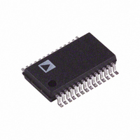
AD976ABRS Analog Devices Inc, AD976ABRS Datasheet - Page 14

AD976ABRS
Manufacturer Part Number
AD976ABRS
Description
IC ADC 16BIT 200KSPS 28-SSOP
Manufacturer
Analog Devices Inc
Datasheet
1.AD976ANZ.pdf
(16 pages)
Specifications of AD976ABRS
Rohs Status
RoHS non-compliant
Number Of Bits
16
Sampling Rate (per Second)
200k
Data Interface
Parallel
Number Of Converters
1
Power Dissipation (max)
100mW
Voltage Supply Source
Analog and Digital
Operating Temperature
-40°C ~ 85°C
Mounting Type
Surface Mount
Package / Case
28-SSOP (0.200", 5.30mm Width)
Number Of Elements
1
Resolution
16Bit
Architecture
SAR
Sample Rate
200KSPS
Input Polarity
Bipolar
Input Type
Voltage
Rated Input Volt
±10V
Differential Input
No
Power Supply Requirement
Analog and Digital
Single Supply Voltage (typ)
5V
Single Supply Voltage (min)
4.75V
Single Supply Voltage (max)
5.25V
Dual Supply Voltage (typ)
Not RequiredV
Dual Supply Voltage (min)
Not RequiredV
Dual Supply Voltage (max)
Not RequiredV
Power Dissipation
100mW
Differential Linearity Error
-1LSB/1.75LSB
Integral Nonlinearity Error
±2LSB
Operating Temp Range
-40C to 85C
Operating Temperature Classification
Industrial
Mounting
Surface Mount
Pin Count
28
Package Type
SSOP
Input Signal Type
Single-Ended
For Use With
EVAL-AD976CB - BOARD EVAL FOR AD976EVAL-AD976ACB - BOARD EVAL FOR AD976A
Lead Free Status / Rohs Status
Not Compliant
Available stocks
Company
Part Number
Manufacturer
Quantity
Price
Part Number:
AD976ABRS
Manufacturer:
ADI/亚德诺
Quantity:
20 000
Part Number:
AD976ABRSZ
Manufacturer:
ADI/亚德诺
Quantity:
20 000
AD976/AD976A
8051 Interface
Figure 21 illustrates the use of the AD976/AD976A with an
8051 microcontroller.
TMS320C25 Interface
Figure 22 shows an interface between the AD976/AD976A and
the TMS320C25.
ADSP-2111 Interface
Figure 23 shows an interface to the ADSP-2111 signal processor.
In this example, CS is being used to control conversions and is
generated by an external timer. A conversion is initiated each
time the timer output goes low as long as you are not reading
from the AD976/AD976A and while the Flag Output (FO) pin
of the ADSP-2111 is low. When a conversion is complete, the
BUSY line will return high. With the IRQn pin programmed to
generate an interrupt on a high-to-low transition, an interrupt
will occur at the end of each conversion. The 16-bit result of the
conversion can be read from within the interrupt service routine
by first forcing FO high, then performing a read operation with
the AD976/AD976A.
Figure 22. AD976/AD976A to TMS320C25 Interface
8051
TMS320C25
P0
P2
AD7
AD0
A15
WR
INT
Figure 21. AD976/AD976A to 8051 Interface
RD
A8
READY
STRB
BUS
NSC
R/W
A15
D15
INT
A0
D0
IS
*ADDITIONAL PINS OMITTED FOR CLARITY
DECODE
LATCH
*ADDITIONAL PINS OMITTED FOR CLARITY
ADDR
BUS
BUS
ADDRESS BUS
DATA BUS
EN
DECODE
A0
ADDR
TIMER
DB15
CS
BUSY
DB0
R/C
AD976A
AD976/
DB0
BYTE
DB7
R/C
CS
BUSY
AD976A
AD976/
–14–
POWER SUPPLIES AND DECOUPLING
The AD976/AD976A has two power supply input pins. V
and V
portions, respectively. V
analog circuitry, and V
digital circuitry. The AD976/AD976A is designed to be inde-
pendent of power supply sequencing and, thus, free from supply
voltage induced latch-up.
With high performance linear circuits, changes in the power
supplies can result in undesired circuit performance. Optimally,
well regulated power supplies should be chosen with less than
1% ripple. The ac output impedance of a power supply is a
complex function of frequency and it will generally increase with
frequency. Thus, high frequency switching, such as that encoun-
tered with digital circuitry, requires the fast transient currents
that most power supplies can not adequately provide. Such a
situation results in large voltage spikes on the supplies. To com-
pensate for the finite ac output impedance of most supplies,
charge “reserves” should be stored in bypass capacitors. This
will effectively lower the supplies impedance presented to the
AD976/AD976A V
of these spikes. Decoupling capacitors, typically 0.1 F, should
be placed close to the power supply pins of the AD976/AD976A
to minimize any inductance between the capacitors and the
V
The AD976/AD976A may be operated from a single +5 V sup-
ply. When separate supplies are used, however, it is beneficial to
have larger capacitors, 10 F, placed between the logic supply
(V
supply (V
10 F capacitors should be located in the vicinity of the ADC to
further reduce low frequency ripple. In systems where the device
will be subjected to harsh environmental noise, additional de-
coupling may be required.
ANA
DIG
Figure 23. AD976/AD976A to ADSP-2111 Interface
ADSP-2111
) and digital common (DGND) and between the analog
and V
DIG
ANA
provide the supply voltages to the analog and digital
DIG
IRQn
DMS
A13
D15
) and the analog common (AGND2). Additionally,
RD
FO
A0
D0
pins.
*ADDITIONAL PINS OMITTED FOR CLARITY
ANA
ADDRESS BUS
EN
DECODE
ADDR
DATA BUS
DIG
and V
ANA
is the +5 V supply for the on-chip
is the +5 V supply for the on-chip
DIG
pins and reduce the magnitude
TIMER
CS
BUSY
DB15
R/C
DB0
AD976A
AD976/
REV. C
ANA


