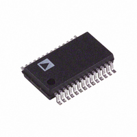
AD976ABRS Analog Devices Inc, AD976ABRS Datasheet - Page 9

AD976ABRS
Manufacturer Part Number
AD976ABRS
Description
IC ADC 16BIT 200KSPS 28-SSOP
Manufacturer
Analog Devices Inc
Datasheet
1.AD976ANZ.pdf
(16 pages)
Specifications of AD976ABRS
Rohs Status
RoHS non-compliant
Number Of Bits
16
Sampling Rate (per Second)
200k
Data Interface
Parallel
Number Of Converters
1
Power Dissipation (max)
100mW
Voltage Supply Source
Analog and Digital
Operating Temperature
-40°C ~ 85°C
Mounting Type
Surface Mount
Package / Case
28-SSOP (0.200", 5.30mm Width)
Number Of Elements
1
Resolution
16Bit
Architecture
SAR
Sample Rate
200KSPS
Input Polarity
Bipolar
Input Type
Voltage
Rated Input Volt
±10V
Differential Input
No
Power Supply Requirement
Analog and Digital
Single Supply Voltage (typ)
5V
Single Supply Voltage (min)
4.75V
Single Supply Voltage (max)
5.25V
Dual Supply Voltage (typ)
Not RequiredV
Dual Supply Voltage (min)
Not RequiredV
Dual Supply Voltage (max)
Not RequiredV
Power Dissipation
100mW
Differential Linearity Error
-1LSB/1.75LSB
Integral Nonlinearity Error
±2LSB
Operating Temp Range
-40C to 85C
Operating Temperature Classification
Industrial
Mounting
Surface Mount
Pin Count
28
Package Type
SSOP
Input Signal Type
Single-Ended
For Use With
EVAL-AD976CB - BOARD EVAL FOR AD976EVAL-AD976ACB - BOARD EVAL FOR AD976A
Lead Free Status / Rohs Status
Not Compliant
Available stocks
Company
Part Number
Manufacturer
Quantity
Price
Part Number:
AD976ABRS
Manufacturer:
ADI/亚德诺
Quantity:
20 000
Part Number:
AD976ABRSZ
Manufacturer:
ADI/亚德诺
Quantity:
20 000
Regardless of the method for controlling conversions, output
data from conversion “n–1” will be valid during the BUSY Low
time for roughly 3.7 s (AD976A only), and output data from
conversion “n” will be valid at the end of a conversion, 50 ns
(t
that data is read only after BUSY goes high since this timing is
much more clearly defined and provides optimal performance.
Figure 4 demonstrates the functionality of the BYTE pin and
shows how the data will be valid in Binary Twos Complement
format only when R/C is asserted High and CS is Low. The
BYTE pin enables the output data on the bus to be read as a
full parallel output or as two 8-bit bytes on Pins 6–13 and Pins
15–22.
ANALOG INPUTS
Figure 5 shows the analog input section for the AD976 when
operating with an internal reference. The analog input range is
nominally a bipolar –10 V to +10 V. Since the AD976/AD976A
can be operated with an internal or external reference, the full-
scale analog input range can be best represented as 4 V
The nominal input impedance is 23 k /13 k with a 22 pF
input capacitance. The analog input section also has a 25 V
overvoltage protection. Since the AD976/AD976A has two
analog grounds it is important to ensure that the analog input is
referenced to the AGND1 pin, the low current ground. This
will minimize any problems associated with a resistive ground
drop. It is also important to ensure that the analog input of the
AD976/AD976A is driven by a low impedance source. With its
primarily resistive analog input circuitry, the ADC can be driven
by a wide selection of general purpose amplifiers.
To best match the low distortion requirements of the AD976/
AD976A, care should be taken in the selection of the drive
circuitry op amp. Figure 6 shows the analog input section for
the AD976A when operating with an internal reference only.
Figure 9 shows the analog input section for both the AD976 and
the AD976A when operating with an external reference.
REV. C
10
) before BUSY returns High. It is recommended, however,
PINS 15–22
PINS 6–13
BYTE
R/C
CS
Figure 4. Using CS and BYTE to Control Data Bus Read Timing
HI-Z
HI-Z
t
12
REF
t
14
HIGH BYTE
LOW BYTE
.
–9–
Figure 5.
Reference)
Figure 6.
Reference) Only
t
14
HIGH BYTE
LOW BYTE
10V INPUT
10V INPUT
10 V Input Connection for the AD976 (Internal
10 V Input Connection for the AD976A (Internal
+5V
33.2k
200
66.4k
200
R1
R1
t
R2
12
R2
t
9
HI-Z
HI-Z
2.2 F
2.2 F
2.2 F
2.2 F
C1
C2
C2
C1
AD976/AD976A
V
AGND1
REF
CAP
AGND2
AGND1
AGND2
V
REF
V
CAP
IN
ANA
IN
AD976A
AD976


