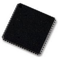
AD9262BCPZ-10 Analog Devices Inc, AD9262BCPZ-10 Datasheet - Page 7

AD9262BCPZ-10
Manufacturer Part Number
AD9262BCPZ-10
Description
IC ADC 16BIT 10MHZ 64LFCSP
Manufacturer
Analog Devices Inc
Datasheet
1.AD9262BCPZRL7.pdf
(32 pages)
Specifications of AD9262BCPZ-10
Data Interface
Serial, SPI™
Design Resources
Interfacing ADL5382 to AD9262 as an RF-to-Bits Solution (CN0062)
Number Of Bits
16
Sampling Rate (per Second)
160M
Number Of Converters
2
Power Dissipation (max)
762mW
Voltage Supply Source
Analog and Digital
Operating Temperature
-40°C ~ 85°C
Mounting Type
Surface Mount
Package / Case
64-LFCSP
Resolution (bits)
16bit
Sampling Rate
160MSPS
Input Channel Type
Differential, Single Ended
Supply Voltage Range - Analog
1.7V To 1.9V
Supply Current
146mA
Lead Free Status / RoHS Status
Lead free / RoHS Compliant
SWITCHING SPECIFICATIONS
All power supplies set to 1.8 V, 640 MHz sample rate, 0.5 V internal reference, PLL disabled, 40 MSPS output data rate, AIN = −2.0 dBFS
unless otherwise noted.
Table 5.
Parameter
CLOCK INPUT (USING CLOCK MULTIPLIER)
CLOCK INPUT (DIRECT CLOCKING)
DATA OUTPUT PARAMETERS
WAKE-UP TIME
OUT-OF-RANGE RECOVERY TIME
SERIAL PORT INTERFACE
1
2
3
4
5
6
Timing Diagram
See the AN-83 5 Application Note, Understanding High Speed ADC Testing and Evaluation, for a complete set of definitions.
Data skew is measured from DCO 50% transition to data (D0x to D15x) 50% transition, with 5 pF load.
Typical measured value for the AD9262BCPZ-10. For the AD9262BCPZ-5 and the AD9262BCPZ, typical values double and quadruple the number of cycles, respectively.
Cycles refers to modulator clock cycles.
Wake-up time is dependent on the value of the decoupling capacitor, value shown with 10uF capacitor on VREF and CFILT.
See Figure 60 and the Serial Port Interface (SPI) section.
Conversion Rate
CLK± Period
CLK± Duty Cycle
Conversion Rate
CLK± Period
CLK± Duty Cycle
Output Data Rate
DCO to Data Skew (t
Sample Latency
Power-Down Power
Standby Power
Sleep Power
SCLK Period
SCLK Pulse Width High Time (t
SCLK Pulse Width Low Time (t
SDIO to SCLK Setup Time (t
SDIO to SCLK Hold Time (t
CSB to SCLK Setup Time (t
CSB to SCLK Hold Time (t
1
5
3
SKEW
6
)
D0x TO D15x
2
SH
SDH
SS
)
SDS
)
)
SLOW
)
3
SHIGH
DCO
)
)
Figure 2. Timing Diagram
Rev. A | Page 7 of 32
Temp
Full
Full
Full
Full
Full
Full
Full
Full
Full
Full
Full
Full
Full
Full
Full
Full
Full
Full
Full
Full
t
SKEW
Min
30
6.25
40
608
1.49
40
20
3
40
16
16
5
2
5
2
Typ
50
640
1.5625
50
960
3
9
15
960
Max
160
33
60
672
1.64
60
160
Unit
MSPS
ns
%
MSPS
ns
%
MSPS
ns
Cycles
μs
μs
μs
Cycles
ns
ns
ns
ns
ns
ns
ns
AD9262
4
4


