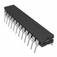
AD7870SQ Analog Devices Inc, AD7870SQ Datasheet - Page 6

AD7870SQ
Manufacturer Part Number
AD7870SQ
Description
IC ADC 12BIT SAMPLING 3V 24-CDIP
Manufacturer
Analog Devices Inc
Datasheet
1.AD7870JNZ.pdf
(28 pages)
Specifications of AD7870SQ
Rohs Status
RoHS non-compliant
Number Of Bits
12
Sampling Rate (per Second)
100k
Data Interface
Serial, Parallel
Number Of Converters
1
Power Dissipation (max)
95mW
Voltage Supply Source
Dual ±
Operating Temperature
-55°C ~ 125°C
Mounting Type
Through Hole
Package / Case
24-CDIP (0.300", 7.62mm)
Available stocks
Company
Part Number
Manufacturer
Quantity
Price
Company:
Part Number:
AD7870SQ/883B
Manufacturer:
NEC
Quantity:
41
AD7870/AD7875/AD7876
TIMING CHARACTERISTICS
V
sample tested at 25°C to ensure compliance, unless otherwise noted. All input signals are specified with t
and timed from a voltage level of 1.6 V.
Table 3.
Parameter
t
t
t
t
t
t
t
t
t
t
t
t
t
t
t
t
t
t
t
t
1
2
3
4
5
6
1
2
3
4
5
6
7
8
9
10
11
12
13
14
15
16
17
18
19
20
Serial timing is measured with a 4.7 kΩ pull-up resistor on SDATA and SSTRB and a 2 kΩ pull-up on SCLK. The capacitance on all three outputs is 35 pF.
Timing specifications for t
t
t
SCLK mark/space ratio (measured from a voltage level of 1.6 V) is 40/60 to 60/40.
SDATA will drive higher capacitive loads but this will add to t
2, 3
2, 4
DD
2
6
7
5
6
is measured with the load circuits of Figure 4 and defined as the time required for an output to cross 0.8 V or 2.4 V.
is defined as the time required for the data lines to change 0.5 V when loaded with the circuits of Figure 5.
= +5 V ± 5%, V
1
Limit at T
(J, K, L, A, B, C Versions)
50
0
60
0
70
57
5
50
0
0
100
370
135
20
100
10
100
60
120
200
0
0
0
SS
= −5 V ± 5%, AGND = DGND = 0 V. See Figure 14, Figure 15, Figure 16, and Figure 17. Timing specifications are
3
, t
6
, and for the maximum limit at t
MIN
, T
MAX
7
12
are 100% production tested.
since it increases the external RC time constant (4.7 kΩ||C
Limit at T
(T Version)
50
0
75
0
70
70
5
50
0
0
100
370
150
20
100
10
100
60
120
200
0
0
0
Rev. C | Page 6 of 28
MIN
, T
MAX
Units
ns min
ns min
ns min
ns min
ns max
ns max
ns min
ns max
ns min
ns min
ns min
ns min
ns max
ns min
ns max
ns min
ns max
ns min
ns max
ns min
ns min
ns min
ns min
Conditions/Comments
CONVST pulse width
CS to RD setup time (Mode 1)
RD pulse width
CS to RD hold time (Mode 1)
RD to INT delay
Data access time after RD
Bus relinquish time after RD
HBEN to RD setup time
HBEN to RD hold time
SSTRB to SCLK falling edge setup time
SCLK cycle time
SCLK to valid data delay. C
SCLK rising edge to SSTRB
Bus relinquish time after SCLK
CS to RD setup time (Mode 2)
CS to BUSY propagation delay
Data setup time prior to BUSY
CS to RD hold time (Mode 2)
HBEN to CS setup time
HBEN to CS hold time
L
) and thus the time to reach 2.4 V.
r
= t
f
= 5 ns (10% to 90% of 5 V)
L
= 35 pF


