ADADC80-Z-12 Analog Devices Inc, ADADC80-Z-12 Datasheet
ADADC80-Z-12
Specifications of ADADC80-Z-12
Available stocks


Related parts for ADADC80-Z-12


ADADC80-Z-12 Summary of contents
Page 1
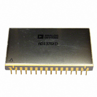
... +10.0 V. The 6.3 V precision reference can be used for external applications. All digital signals are fully DTL and TTL compatible; output data is in parallel form. The ADADC80 is available in grades specified for use over the −25°C to +85°C temperature range and is available in a 32-lead ceramic DIP. ...
Page 2
... ADADC80 TABLE OF CONTENTS Features .............................................................................................. 1 Functional Block Diagram .............................................................. 1 Product Description ......................................................................... 1 Product Highlights ........................................................................... 1 Revision History ............................................................................... 2 Specifications ..................................................................................... 3 Absolute Maximum Ratings ............................................................ 5 ESD Caution .................................................................................. 5 Pin Configuration and Function Descriptions ............................. 6 Typical Performance Characteristics ............................................. 7 Theory of Operation ........................................................................ 8 REVISION HISTORY 2/08—Rev Rev. E Updated Format .................................................................. Universal Pin 7 Changed to NC ......................................................... Universal Changes to Specifications Section ...
Page 3
... Guaranteed 17 22 COB, CTC CSB 2 Logic 1 during conversion 2 2 575 Rev Page ADADC80 Max Unit Bits V V kΩ kΩ kΩ ns TTL load TTL load FSR % of FSR % of FSR ±0.012 % of FSR LSB LSB +85 ° ...
Page 4
... Guaranteed by design. Not production tested. 6 Conversion time with internal clock. 7 See Table 4. Complementary offset binary is COB, complementary straight binary is CSB, and complementary twos complement is CTC. 8 For conversion speeds specified. 9 For “Z” models, order ADADC80-Z-12. Min Typ ±10 1.5 ±10 ±15, +5 +4.75 ± ...
Page 5
... V other conditions above those indicated in the operational ±0.3 V section of this specification is not implied. Exposure to absolute ±V S maximum rating conditions for extended periods may affect −0 0 device reliability. 175°C 150°C 300°C ESD CAUTION Rev Page ADADC80 ...
Page 6
... REF OUT (6.3V) 25 −15V OR −12V BIT 12 (LSB) to BIT 7 BIT 6 BIT BIT 5 2 BIT 8 31 BIT BIT 9 BIT 3 BIT ADADC80 BIT 2 BIT TOP VIEW BIT 1 (MSB) (Not to Scale) BIT 12 (LSB BIT 1 (MSB) –15V OR –12V DIGITAL SUPPLY REF OUT (6.3V DIGITAL GND CLOCK OUT ...
Page 7
... Figure 4. Gain Drift Error vs. Temperature 1.00 0.75 0.50 0. Figure 5. Differential Linearity Error vs. Conversion Time (Normalized) 0.08 0.06 0.04 0.02 –0.02 –0.04 –0.06 –0. Rev Page 8-BIT 10-BIT 12-BIT CONVERSION TIME (µs) 0 TYPICAL –55 – TEMPERATURE (°C) Figure 6. Reference Drift, Error vs. Temperature ADADC80 100 ...
Page 8
... ADADC80 THEORY OF OPERATION Upon receipt of a CONVERT START command, the ADADC80 converts the voltage at its analog input into an equivalent 12-bit binary number. This conversion is accomplished as follows: 1. The 12-bit successive-approximation register (SAR) has its 12-bit outputs connected both to the device bit output pins and to the corresponding bit inputs of the feedback DAC ...
Page 9
... SHORT CYCLE (Pin 21) is connected to 5V DIGITAL SUPPLY (Pin 9). INPUT SCALING The ADADC80 input should be scaled as close to the maximum input signal range as possible to use the maximum signal resolution of the ADC. Connect the input signal as shown in Table 5. See Figure 8 for circuit details. ...
Page 10
... GAIN ADADC80 TO 16 ADJUST 100kΩ 0.01µF –15V Figure 11. Gain Adjustment Circuit +15V 270kΩ 270kΩ GAIN 10kΩ ADJUST ADADC80 TO 16 100kΩ 6.8kΩ 0.1µF –15V Figure 12. Low Tempco Gain Adjustment Circuit CSB 19.53 mV 4. − ...
Page 11
... OUT IN ADJUST –15V 10MΩ ANALOG 10kΩ INPUT 0.01µF +15V Rev Page SAR DAC 10V SPAN COMPARATOR COMPARATOR –15V 1.8MΩ 10kΩ +15V ANALOG INPUT SAR DAC 10V SPAN COMPARATOR COMPARATOR –15V 1.8MΩ 10kΩ +15V ADADC80 ...
Page 12
... Each of the ADADC80 supply terminals should be capacitively decoupled as close to the ADADC80 as possible. A large value capacitor, such as 1 μF in parallel with a 0.1 μF capacitor, is usually sufficient. Analog supplies are bypassed to the analog power return pin, and the logic supply is bypassed to the logic power return pin ...
Page 13
... CONTROL MODES The timing sequence of the ADADC80 allows the device to be easily operated in a variety of systems with different control modes. The most common control modes are illustrated in Figure 16, Figure 17, and Figure 18. ADADC80 CONVERT 18 BIT 11 28 START CONVERT COMMAND SHORT 21 CYCLE CLOCK ...
Page 14
... PARENTHESES) ARE ROUNDED-OFF INCH EQUIVALENTS FOR REFERENCE ONLY AND ARE NOT APPROPRIATE FOR USE IN DESIGN. ORDERING GUIDE Model Temperature Range ADADC80-12 –25°C to +85°C ADADC80-Z-12 1 –25°C to +85°C 1 “Z “= Models for ±12 V supplies. This part is not RoHS compliant. SEE NOTE 4 0.098 (2.49) MAX 17 0 ...
Page 15
... NOTES Rev Page ADADC80 ...
Page 16
... ADADC80 NOTES ©2002–2008 Analog Devices, Inc. All rights reserved. Trademarks and registered trademarks are the property of their respective owners. D01202-0-2/08(E) Rev Page ...