ADADC80-Z-12 Analog Devices Inc, ADADC80-Z-12 Datasheet - Page 9
ADADC80-Z-12
Manufacturer Part Number
ADADC80-Z-12
Description
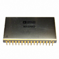
IC ADC 12BIT INTEGRATED 32-CDIP
Manufacturer
Analog Devices Inc
Datasheet
1.ADADC80-12.pdf
(16 pages)
Specifications of ADADC80-Z-12
Data Interface
Parallel
Number Of Bits
12
Sampling Rate (per Second)
40k
Number Of Converters
1
Power Dissipation (max)
800mW
Voltage Supply Source
Analog and Digital, Dual ±
Operating Temperature
-25°C ~ 85°C
Mounting Type
Through Hole
Package / Case
32-CDIP (0.900", 22.86mm)
Resolution (bits)
12bit
Input Channel Type
Single Ended
Supply Current
70mA
Digital Ic Case Style
DIP
No. Of Pins
32
Operating Temperature Range
-25°C To +85°C
Lead Free Status / RoHS Status
Lead free / RoHS non-compliant
Available stocks
Company
Part Number
Manufacturer
Quantity
Price


DIGITAL OUTPUT DATA
Parallel data from TTL storage registers is in negative true form.
Parallel data output coding is complementary binary for
unipolar ranges and either complementary offset binary or
complementary twos complement binary for bipolar ranges,
depending on whether BIT 1 (Pin 6) or its logical inverse
BIT 1 (MSB) (Pin 8) is used as the MSB. Parallel data becomes
valid approximately 40 ns before the STATUS flag returns to
Logic 0, permitting parallel data transfer to be clocked on the
1 to 0 transition of the STATUS flag.
Parallel data outputs change state on positive-going clock edges.
There are 13 negative-going clock edges in the complete 12-bit
conversion cycle, as shown in Figure 7. The first edge shifts an
invalid bit into the register, which is shifted out on the 13th
negative-going clock edge.
SHORT CYCLE Input
The SHORT CYCLE input (Pin 21) permits the timing cycle shown
in Figure 7 to be terminated after any number of desired bits has
been converted, allowing somewhat shorter conversion times in
applications not requiring full 12-bit resolution. When 10-bit
resolution is desired, Pin 21 is connected to the BIT 11 output
(Pin 28). The conversion cycle then terminates, and the
STATUS flag resets after the BIT 10 decision (t
Table 4. Short Cycle Connections
Connect SHORT CYCLE (Pin 21) to
5V DIGITAL SUPPLY (Pin 9)
BIT 11 (Pin 28)
BIT 9 (Pin 30)
Table 5. Input Scaling Connections
Input Signal Range
±10 V
±5 V
±2.5 V
0 V to +5 V
0 V to +10 V
Output Code
COB or CTC
COB or CTC
COB or CTC
CSB
CSB
Connect BIPOLAR OFFSET OUT
(Pin 12) to
COMPARATOR IN (Pin 11)
COMPARATOR IN (Pin 11)
COMPARATOR IN (Pin 11)
ANALOG GND (Pin 15)
ANALOG GND (Pin 15)
Resolution (Bits)
12
10
8
10
+ 40 ns in timing
Rev. E | Page 9 of 16
(% FSR)
0.024
0.100
0.390
diagram of Figure 7). Short cycle pin connections and
associated maximum 12-, 10-, and 8-bit conversion times are
summarized in Table 4. When 12-bit resolution is required,
SHORT CYCLE (Pin 21) is connected to 5V DIGITAL SUPPLY
(Pin 9).
INPUT SCALING
The ADADC80 input should be scaled as close to the maximum
input signal range as possible to use the maximum signal
resolution of the ADC. Connect the input signal as shown in
Table 5. See Figure 8 for circuit details.
Maximum Conversion Time (μs)
25
21
17
Connect 20V SPAN IN
(Pin 14) to
Input Signal
Open
COMPARATOR IN (Pin 11)
COMPARATOR IN (Pin 11)
Open
COMPARATOR IN
OFFSET OUT
10V SPAN IN
20V SPAN IN
BIPOLAR
ANALOG
GND
Figure 8. Input Scaling Circuit
13
14
11
12
15
6.3kΩ
FROM
DAC
5kΩ
R2
V
REF
R1
5kΩ
Connect Input Signal to
20V SPAN IN (Pin 14)
10V SPAN IN (Pin 13)
10V SPAN IN (Pin 13)
10V SPAN IN (Pin 13)
10V SPAN IN (Pin 13)
COMPARATOR
STATUS Flag Reset
t
t
t
12
10
8
+ 40 ns
+ 40 ns
+ 40 ns
ADADC80
TO SAR
Related parts for ADADC80-Z-12
Image
Part Number
Description
Manufacturer
Datasheet
Request
R

Part Number:
Description:
IC ADC 12-BIT INTEGRATED 32-CDIP
Manufacturer:
Analog Devices Inc
Datasheet:

Part Number:
Description:
±1.7g Dual-Axis IMEMS Accelerometer Evaluation Board
Manufacturer:
Analog Devices Inc
Datasheet:

Part Number:
Description:
Inertial Sensor Evaluation System
Manufacturer:
Analog Devices Inc
Datasheet:
Part Number:
Description:
Manufacturer:
Analog Devices Inc
Datasheet:
Part Number:
Description:
Manufacturer:
Analog Devices Inc
Datasheet:
Part Number:
Description:
Manufacturer:
Analog Devices Inc
Datasheet:
Part Number:
Description:
Manufacturer:
Analog Devices Inc
Datasheet:
Part Number:
Description:
Manufacturer:
Analog Devices Inc
Datasheet:
Part Number:
Description:
Manufacturer:
Analog Devices Inc
Datasheet:
Part Number:
Description:
Manufacturer:
Analog Devices Inc
Datasheet:
Part Number:
Description:
Manufacturer:
Analog Devices Inc
Datasheet:
Part Number:
Description:
Manufacturer:
Analog Devices Inc
Datasheet:
Part Number:
Description:
Manufacturer:
Analog Devices Inc
Datasheet: