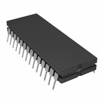
AD7871TQ Analog Devices Inc, AD7871TQ Datasheet - Page 11

AD7871TQ
Manufacturer Part Number
AD7871TQ
Description
IC ADC 14BIT SAMPLING 28-CDIP
Manufacturer
Analog Devices Inc
Datasheet
1.AD7872JRZ-REEL.pdf
(16 pages)
Specifications of AD7871TQ
Rohs Status
RoHS non-compliant
Number Of Bits
14
Sampling Rate (per Second)
83k
Data Interface
Serial, Parallel
Number Of Converters
1
Power Dissipation (max)
95mW
Voltage Supply Source
Dual ±
Operating Temperature
-55°C ~ 125°C
Mounting Type
Through Hole
Package / Case
28-CDIP (0.600", 15.24mm)
Using the CCIF standard where two input frequencies near the
top end of the input bandwidth are used, the second and third or-
der terms are of different significance. The second order terms
are usually distanced in frequency from the original sine waves
while the third order terms are usually at a frequency close to the
input frequencies. As a result, the second and third order terms
are specified separately. The calculation of the intermodulation
distortion is as per the THD specification where it is the ratio of
the rms sum of the individual distortion products to the rms
amplitude of the fundamental expressed in dBs. In this case, the
input consists of two, equal amplitude, low distortion sine waves.
Figure 16 shows a typical IMD plot for the AD7871/AD7872.
Peak Harmonic or Spurious Noise
Peak Harmonic or Spurious Noise is defined as the ratio of the
rms value of the next largest component in the ADC output
spectrum (up to fs/2 and excluding dc) to the rms value of the
fundamental. Normally, the value of this specification will be
determined by the largest harmonic in the spectrum, but for
parts where the harmonics are buried in the noise floor, peak
will be a noise peak.
MICROPROCESSOR INTERFACE
The AD7871 and AD7872 have a wide variety of interfacing op-
tions. The AD7871 offers two operating modes and three
data-output formats, while the AD7872 is a dedicated serial
output device. The fast data access times on the parallel modes
of the AD7871 allow interfacing to the very fast DSPs. The se-
rial mode on both the AD7871 and AD7872 is compatible with
the serial port structures on all the popular DSPs.
Parallel Read Interfacing
Figures 17 and 18 show interfaces to the ADSP-2100 and the
TMS32020/C25 DSP processors. The AD7871 is operating in
Mode 1, parallel read for both interfaces. An external timer con-
trols conversion start asynchronously to the microprocessor. At
the end of each conversion the ADC BUSY/INT interrupts the
REV. D
Figure 16. IMD Plot
–11–
microprocessor and the conversion result is read from the ADC
with the following instruction:
Some applications may require that conversions be initiated by
the microprocessor rather than an external timer. One option is
to decode the AD7871 CONVST from the address bus so that a
write operation to the ADC starts a conversion. Data is read at
the end of conversion as described earlier. Note, a read opera-
tion must not be attempted during conversion.
ADSP-2100 MR0 = DM(ADC)
TMS32020/C25: IN D,ADC
MR0 = ADSP-2100 MR0 Register
D = Data Memory Address
ADC = AD7871 Address
Figure 17. AD7871 to ADSP-2100 Parallel Interface
Figure 18. AD7871 to TMS32020/C25 Interface
AD7871/AD7872


