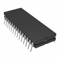
AD7871TQ Analog Devices Inc, AD7871TQ Datasheet - Page 4

AD7871TQ
Manufacturer Part Number
AD7871TQ
Description
IC ADC 14BIT SAMPLING 28-CDIP
Manufacturer
Analog Devices Inc
Datasheet
1.AD7872JRZ-REEL.pdf
(16 pages)
Specifications of AD7871TQ
Rohs Status
RoHS non-compliant
Number Of Bits
14
Sampling Rate (per Second)
83k
Data Interface
Serial, Parallel
Number Of Converters
1
Power Dissipation (max)
95mW
Voltage Supply Source
Dual ±
Operating Temperature
-55°C ~ 125°C
Mounting Type
Through Hole
Package / Case
28-CDIP (0.600", 15.24mm)
AD7871/AD7872
AD7871 PIN FUNCTION DESCRIPTION
DIP
No.
1
2
3
4
5
6
7
8
9
10–13 DB9–DB6
14
15–20 DB5/DB13–
21
22
23
24
25
26
27
28
Mnemonic
CONVST
CS
RD
BUSY/INT
CLK
DB13/HBEN
DB12/SSTRB
DB11/SCLK
DB10/SDATA
DGND
DB0/DB8
V
AGND
C
NC
REF OUT
V
V
14/8/CLK
DD
IN
SS
REF
either byte or serial data is selected, this pin becomes the HBEN logic input. HBEN is used for 8-bit
bus interfacing. When HBEN is low, DB7 to DB0 is the lower byte of data. With HBEN high, DB7
to DB0 is the upper byte of data (see Table I).
Three-State Data Outputs controlled by CS and RD. Their function depends on the state of the
Function
Convert Start. A low to high transition on this input puts the track/hold into the hold mode. This
input is asynchronous to the CLK. CS and RD must be held high for the duration of this pulse.
Chip Select. Active low logic input. The device is selected when this input is active. With CONVST
tied low, a new conversion is initiated when CS goes low.
Read. Active low logic input. This input is used in conjunction with CS low to enable the data outputs.
Busy/Interrupt. Logic low output indicating converter status. See timing diagrams.
Clock Input. An external TTL-compatible clock may be applied to this input. Alternatively, tying
this pin to V
Data Bit 13 (MSB)/High Byte Enable. The function of this pin is dependent on the state of the
14/8/CLK input (see Pin 28). When 14-bit data is selected, this pin provides the DB13 output. When
Data Bit 12/Serial Strobe. When 14-bit data is selected, this pin provides the DB12 data output.
Otherwise it is an active low three-state output that provides a framing pulse for serial data.
Data Bit 11/Serial Clock. When 14-bit data is selected, this pin provides the DB11 data output.
Otherwise SCLK is the gated serial clock output that is derived from the internal or external ADC
clock. If the 14/8/CLK input is held at –5 V, then the SCLK runs continuously. With 14/8/CLK at
0 V, it is gated off (three-state) after serial transmission is complete.
Data Bit 10/Serial Data. When 14-bit parallel data is selected, this pin provides the DB10 data
output. Otherwise it is the three-state serial data output used in conjunction with SCLK and SSTRB
in serial data transmission. Serial data is valid on the falling edge of SCLK, when SSTRB is low.
14/8/CLK and the HBEN inputs. With 14/8/CLK high, they are always DB9–DB6; with 14/8/CLK
low, their function depends on HBEN (see Table I).
Digital Ground. Ground return for digital circuitry.
Three-State Data Outputs controlled by CS and RD. Their function depends on the 14/8/CLK
and HBEN inputs. With 14/8/CLK high, they are always DB5–DB0; with 14/8/CLK low or –5 V,
their function is controlled by HBEN (see Table I).
Positive Supply, +5 V
Analog Ground. Ground reference for analog circuitry.
Decoupling point for on-chip reference. Connect 10 nF between this pin and AGND.
No Connect.
Voltage Reference Output. The internal 3 V reference is provided at this pin. The external load
capability is 500 A.
Analog Input. The input range is 3 V.
Negative Supply, –5 V
Three-Function Input. Defines both the parallel and serial data formats. With this pin at +5 V, the
output data is 14-bit parallel only. With this pin at 0 V, both byte and serial data are available, and
the SCLK is noncontinuous. With this pin at –5 V, both byte and serial data are available and the
SCLK is continuous.
HBEN DB7
HIGH LOW LOW DB13 DB12 DB11 DB10 DB9 DB8
LOW
SS
enables the internal laser-trimmed oscillator.
DB7
DB6 DB5 DB4 DB3 DB2
DB6 DB5 DB4 DB3 DB2
5%.
Table I. Byte Output Format
5%.
–4–
DB1 DB0
DB1 DB0
REV. D


