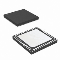
KAD5514P-12Q48 Intersil, KAD5514P-12Q48 Datasheet - Page 18

KAD5514P-12Q48
Manufacturer Part Number
KAD5514P-12Q48
Description
IC ADC 14BIT 125MSPS SGL 48-QFN
Manufacturer
Intersil
Series
FemtoCharge™r
Datasheet
1.KAD5514P-25Q72.pdf
(34 pages)
Specifications of KAD5514P-12Q48
Number Of Bits
14
Sampling Rate (per Second)
125M
Data Interface
Serial, SPI™
Number Of Converters
1
Power Dissipation (max)
376mW
Voltage Supply Source
Single Supply
Operating Temperature
-40°C ~ 85°C
Mounting Type
Surface Mount
Package / Case
48-VQFN
For Use With
KDC5514-Q48EVAL - DAUGHTER CARD FOR KAD5514KDC5514EVALZ - DAUGHTER CARD FOR KAD5514
Lead Free Status / RoHS Status
Lead free / RoHS Compliant
The calibration sequence is initiated on the rising edge of
RESETN, as shown in Figure 24. The over-range output
(OR) is set high once RESETN is pulled low, and remains in
that state until calibration is complete. The OR output returns
to normal operation at that time, so it is important that the
analog input be within the converter’s full-scale range to
observe the transition. If the input is in an over-range
condition the OR pin will stay high, and it will not be possible
to detect the end of the calibration cycle.
While RESETN is low, the output clock
(CLKOUTP/CLKOUTN) is set low. Normal operation of the
output clock resumes at the next input clock edge
(CLKP/CLKN) after RESETN is deasserted. At 250MSPS
the nominal calibration time is 200ms, while the maximum
calibration time is 550ms.
CLKOUTP
User-Initiated Reset
Recalibration of the ADC can be initiated at any time by
driving the RESETN pin low for a minimum of one clock
cycle. An open-drain driver with a drive strength of less than
0.5mA is recommended, RESETN has an internal high
impedance pull-up to OVDD. As is the case during power-on
reset, the SDO, RESETN and DNC pins must be in the
proper state for the calibration to successfully execute.
The performance of the KAD5514P changes with variations
in temperature, supply voltage or sample rate. The extent of
these changes may necessitate recalibration, depending on
system performance requirements. Best performance will be
achieved by recalibrating the ADC under the environmental
conditions at which it will operate.
RESETN
CLKN
CLKP
ORP
FIGURE 24. CALIBRATION TIMING
CALIBRATION
BEGINS
18
CALIBRATION
CALIBRATION
COMPLETE
TIME
KAD5514P
A supply voltage variation of less than 100mV will generally
result in an SNR change of less than 0.5dBFS and SFDR
change of less than 3dBc. In situations where the sample
rate is not constant, best results will be obtained if the device
is calibrated at the highest sample rate. Reducing the
sample rate by less than 80MSPS will typically result in an
SNR change of less than 0.5dBFS and an SFDR change of
less than 3dBc.
Figures 25 and 26 show the effect of temperature on SNR
and SFDR performance with calibration performed at -
40°C,+25°C, and +85°C. Each plot shows the variation of
SNR/SFDR across temperature after a single calibration at
-40°C, +25°C and +85°C. Best performance is typically
achieved by a user-initiated calibration at the operating
conditions, as stated earlier. However, it can be seen that
performance drift with temperature is not a very strong
function of the temperature at which the calibration is
performed. Full-rated performance will be achieved after
power-up calibration regardless of the operating conditions.
FIGURE 26. SFDR PERFORMANCE vs TEMPERATURE
FIGURE 25. SNR PERFORMANCE vs TEMPERATURE
-10
-15
-1
-2
-3
-4
15
10
3
2
1
0
-40
-5
5
0
-40
-15
-15
CAL DONE AT
CAL DONE AT
-40°C
CAL DONE AT
CAL DONE AT
TEMPERATURE (°C)
TEMPERATURE (°C)
-40°C
10
+85°C
+85°C
10
35
35
CAL DONE AT
CAL DONE AT
+25°C
+25°C
September 10, 2009
60
60
FN6804.2
85
85


