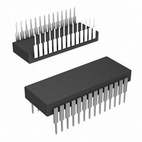
HI1-674AKD-5 Intersil, HI1-674AKD-5 Datasheet - Page 13

HI1-674AKD-5
Manufacturer Part Number
HI1-674AKD-5
Description
IC ADC 12BIT 67KSPS 1CH 28-SBDIP
Manufacturer
Intersil
Datasheet
1.HI3-574AKN-5Z.pdf
(18 pages)
Specifications of HI1-674AKD-5
Number Of Bits
12
Sampling Rate (per Second)
67k
Data Interface
Parallel
Number Of Converters
1
Power Dissipation (max)
720mW
Voltage Supply Source
Dual ±
Operating Temperature
0°C ~ 75°C
Mounting Type
Through Hole
Package / Case
28-CDIP (0.600", 15.24mm)
Lead Free Status / RoHS Status
Lead free / RoHS Compliant
Available stocks
Company
Part Number
Manufacturer
Quantity
Price
Conversion Start
A conversion may be initiated as shown in Table 3 by a logic
transition on any of three inputs: CE, CS or R/C. The last of
the three to reach the correct state starts the conversion, so
one, two or all three may be dynamically controlled. The
nominal delay from each is the same, and if necessary, all
three may change state simultaneously. However, to ensure
that a particular input controls the start of conversion, the
other two should be set up at least 50ns earlier. See the
HI-X74A Timing Specifications, Convert Mode.
This variety of HI-X74A control modes allows a simple
interface in most system applications. The Convert Start
timing relationships are illustrated in Figure 3.
The output signal STS indicates status of the converter by
going high only while a conversion is in progress. While STS
is high, the output buffers remain in a high impedance state
and data cannot be read. Also, an additional Start Convert
will not reset the converter or re-initiate a conversion while
STS is high.
Reading the Output Data
The output data buffers remain in a high impedance state
until four conditions are met: R/C high, STS low, CE high
and CS low. At that time, data lines become active according
to the state of inputs 12/8 and A
illustrated in Figure 4.
The 12/8 input will be tied high or low in most applications,
though it is fully TTL/CMOS-compatible. With 12/8 high, all
DB11-DB0
See HI-X74A Timing Specifications for more information.
STS
R/C
CE
CS
A
O
t
t
SSC
t
SRC
FIGURE 3. CONVERT START TIMING
SAC
t
HRC
t
HAC
t
DSC
HIGH IMPEDANCE
13
O
t
t
. Timing constraints are
HEC
HSC
t
C
HI-574A, HI-674A
•
12 output lines become active simultaneously, for interface
to a 12-bit or 16-bit data bus. The A
With 12/8 low, the output is organized in two 8-bit bytes,
selected one at a time by A
to be connected as shown in Figure 5. A
the least significant bit of the address bus, for storing the
HI-X74A output in two consecutive memory locations. (With
A
are disabled, bits 4 through 7 are forced low, and the 4 LSBs
are enabled). This two byte format is considered “left justified
data,” for which a decimal (or binary!) point is assumed to
the left of byte 1:
Further, A
the converter. Break-before-make action is guaranteed
between the two data bytes, which assures that the outputs
strapped together in Figure 5 will never be enabled at the
same time.
A read operation usually begins after the conversion is
complete and STS is low. For earliest access to the data,
however, the read should begin no later than (t
before STS goes low. See Figure 4.
DB11-DB0
O
MSB
X
low, the 8 MSBs only are enabled. With A
See HI-X74A Timing Specifications for more information.
STS
R/C
X
A
CE
CS
O
X
O
may be toggled at any time without damage to
BYTE 1
X
FIGURE 4. READ CYCLE TIMING
X
X
X
HIGH IMPEDANCE
O
X
t
t
t
. This allows an 8-bit data bus
SRR
SAR
SSR
t
DD
t
HS
X
O
X
t
t
t
input is ignored.
HSR
HRR
HAR
X
O
LSB
BYTE 2
is usually tied to
VALID
X
DATA
O
high, 4 MSBs
DD
0
August 7, 2008
+ t
0
t
HL
t
HS
HD
FN3096.6
0
)
0


