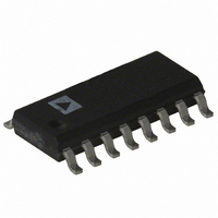
AD7888AR-REEL7 Analog Devices Inc, AD7888AR-REEL7 Datasheet - Page 15

AD7888AR-REEL7
Manufacturer Part Number
AD7888AR-REEL7
Description
IC ADC 12BIT 8CH SRL 16-SOIC
Manufacturer
Analog Devices Inc
Datasheet
1.AD7888ARZ.pdf
(17 pages)
Specifications of AD7888AR-REEL7
Rohs Status
RoHS non-compliant
Number Of Bits
12
Sampling Rate (per Second)
125k
Data Interface
DSP, MICROWIRE™, QSPI™, Serial, SPI™
Number Of Converters
1
Power Dissipation (max)
3.5mW
Voltage Supply Source
Single Supply
Operating Temperature
-40°C ~ 105°C
Mounting Type
Surface Mount
Package / Case
16-SOIC (0.154", 3.90mm Width)
REV. C
AD7888 to MC68HC11
The Serial Peripheral Interface (SPI) on the MC68HC11 is
configured for Master Mode (MSTR = 1), Clock Polarity Bit
(CPOL) = 1 and the Clock Phase Bit (CPHA) = 1. The SPI is
configured by writing to the SPI Control Register (SPCR)—see
68HC11 User Manual. The serial transfer will take place as two
8-bit operations. A connection diagram is shown in Figure 20.
AD7888 to 8051
It is possible to implement a serial interface using the data
ports on the 8051. This allows a full duplex serial transfer to be
implemented. The technique involves “bit-banging” an I/O port
(e.g., P1.0) to generate a serial clock and using two other I/O
ports (e.g., P1.1 and P1.2) to shift data in and out—see
Figure 21.
AD7888 to PIC16C6x/7x
The PIC16C6x Synchronous Serial Port (SSP) is configured
as an SPI Master with the Clock Polarity Bit = 1. This is done
by writing to the Synchronous Serial Port Control Register
(SSPCON). See user PIC16/17 Microcontroller User Manual.
Figure 22 shows the hardware connections needed to interface
to the PIC16/17. In this example I/O port RA1 is being used to
pulse CS. This microcontroller only transfers eight bits of data
during each serial transfer operation. Therefore, two consecutive
read/write operations are needed.
ADDITIONAL PINS OMITTED FOR CLARITY
ADDITIONAL PINS OMITTED FOR CLARITY
ADDITIONAL PINS OMITTED FOR CLARITY
AD7888
AD7888
AD7888
DOUT
SCLK
DOUT
DOUT
SCLK
SCLK
DIN
DIN
DIN
CS
CS
CS
SCK/RC3
SDO/RC5
SDI/RC4
RA1
P1.0
P1.1
P1.2
P1.3
SCLK/PD4
MISO/PD2
MOSI/PD3
PA0
PIC16C6x/7x
MC68HC11
8051
APPLICATION HINTS
Grounding and Layout
The AD7888 has very good immunity to noise on the power
supplies as can be seen by the PSRR vs. Frequency graph.
However, care should still be taken with regard to grounding
and layout.
The printed circuit board that houses the AD7888 should be
designed so the analog and digital sections are separated and
confined to certain areas of the board. This facilitates the use of
ground planes that can be easily separated. A minimum etch
technique is generally best for ground planes as it gives the best
shielding. Digital and analog ground planes should be joined in
only one place. Both AGND pins of the AD7888 should be
sunk in the AGND plane. The AGND plane and DGND plane
connection should be made at one point only, a star ground
point that should be established as close as possible to an AGND
pin of the AD7888.
Avoid running digital lines under the device as these will couple
noise onto the die. The analog ground plane should be allowed
to run under the AD7888 to avoid noise coupling. The power
supply lines to the AD7888 should use as large a trace as pos-
sible to provide low impedance paths and reduce the effects of
glitches on the power supply line. Fast switching signals like
clocks should be shielded with digital ground to avoid radiating
noise to other sections of the board, and clock signals should
never be run near the analog inputs. Avoid crossover of digital
and analog signals. Traces on opposite sides of the board should
run at right angles to each other. This will reduce the effects of
feedthrough through the board. A microstrip technique is by far
the best but is not always possible with a double-sided board. In
this technique, the component side of the board is dedicated to
ground planes while signals are placed on the solder side.
Good decoupling is also important. All analog supplies should
be decoupled with 10 µF tantalum in parallel with 0.1 µF capaci-
tors to AGND. To achieve the best from these decoupling
components, they must be placed as close as possible to the
device, ideally right up against the device.
Evaluating the AD7888 Performance
The recommended layout for the AD7888 is outlined in the
evaluation board for the AD7888. The evaluation board pack-
age includes a fully assembled and tested evaluation board,
documentation, and software for controlling the board from the
PC via the EVAL-CONTROL BOARD. The EVAL-CONTROL
BOARD can be used in conjunction with the AD7888 evalua-
tion board, as well as many other Analog Devices evaluation
boards ending in the CB designator, to demonstrate/evaluate
the ac and dc performance of the AD7888.
The software allows the user to perform ac (fast Fourier trans-
form) and dc (histogram of codes) tests on the AD7888.
AD7888


