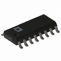
AD7888AR-REEL7 Analog Devices Inc, AD7888AR-REEL7 Datasheet - Page 8

AD7888AR-REEL7
Manufacturer Part Number
AD7888AR-REEL7
Description
IC ADC 12BIT 8CH SRL 16-SOIC
Manufacturer
Analog Devices Inc
Datasheet
1.AD7888ARZ.pdf
(17 pages)
Specifications of AD7888AR-REEL7
Rohs Status
RoHS non-compliant
Number Of Bits
12
Sampling Rate (per Second)
125k
Data Interface
DSP, MICROWIRE™, QSPI™, Serial, SPI™
Number Of Converters
1
Power Dissipation (max)
3.5mW
Voltage Supply Source
Single Supply
Operating Temperature
-40°C ~ 105°C
Mounting Type
Surface Mount
Package / Case
16-SOIC (0.154", 3.90mm Width)
AD7888
Figure 4 shows the typical power supply rejection ratio vs.
frequency for the part. The power supply rejection ratio is defined
as the ratio of the power in the ADC output at frequency f
to the power of a full-scale sine wave applied to the ADC of
frequency fs:
Pf = Power at frequency f in ADC output, Pfs = power at fre-
quency fs in ADC full scale input. Here a 100 mV peak-to-peak
sine wave is coupled onto the V
5.5 V supply performances are shown.
CIRCUIT INFORMATION
The AD7888 is a fast, low power, 12-bit, single supply, 8-channel
A/D converter. The part can be operated from 3 V (2.7 V to
3.6 V) supply or from 5 V (4.75 V to 5.25 V) supply. When
operated from either a 5 V supply or a 3 V supply, the AD7888
is capable of throughput rates of 125 kSPS when provided with
a 2 MHz clock.
The AD7888 provides the user with an 8-channel multiplexer,
on-chip track/hold, A/D converter, reference and serial interface
housed in a tiny 16-lead TSSOP package, which offers the user
considerable space saving advantages over alternative solutions.
The serial clock input accesses data from the part and also
provides the clock source for the successive-approximation
A/D converter. The analog input range is 0 to V
the externally-applied V
The 8-channel multiplexer is controlled by the part’s Control
Register. This Control Register also allows the user to power-off
the internal reference and to determine the Modes of Operation.
CONVERTER OPERATION
The AD7888 is a successive-approximation analog-to-digital
converter based around a charge redistribution DAC. Figures 5
and 6 show simplified schematics of the ADC. Figure 5 shows
the ADC during its acquisition phase. SW2 is closed and SW1 is
in Position A, the comparator is held in a balanced condition
and the sampling capacitor acquires the signal on AIN.
–75
–77
–79
–81
–83
–85
–87
–89
–91
–93
2.65
V
100mV p-p SINE WAVE ON V
REF
DD
IN
12.85
= 5.5V/2.7V
PSRR (dB) = 10 log (Pf/Pfs)
= 2.488V EXT REFERENCE
REF
23.15
INPUT FREQUENCY – kHz
can be between 1.2 V and V
DD
33.65
DD
supply. Both the 2.7 V and
43.85
54.35
REF
(where
64.15
DD
).
When the ADC starts a conversion, (see Figure 6), SW2 will open
and SW1 will move to Position B causing the comparator to
become unbalanced. The control logic and the charge redistribu-
tion DAC are used to add and subtract fixed amounts of charge
from the sampling capacitor to bring the comparator back into a
balanced condition. When the comparator is rebalanced, the
conversion is complete. The control logic generates the ADC
output code. Figure 7 shows the ADC transfer function.
ADC TRANSFER FUNCTION
The output coding of the AD7888 is straight binary. The
designed code transitions occur at successive integer LSB
values (i.e., 1 LSB, 2 LSBs, etc.). The LSB size is = V
4096. The ideal transfer characteristic for the AD7888 is
shown in Figure 7 below.
AIN
VIN
AGND
AGND
(REF IN/REF OUT)/2
(REF IN/REF OUT)/2
A
SW1
A
SW1
000...010
000...001
000...000
111...111
111...110
111...000
011...111
B
B
CAPACITOR
ACQUISITION
0V
SAMPLING
CAPACITOR
CONVERSION
SAMPLING
PHASE
0.5LSB
PHASE
SW2
SW2
ANALOG INPUT
1LSB = V
COMPARATOR
COMPARATOR
REF
+V
/4096
REF
REDISTRIBUTION
REDISTRIBUTION
– 1.5LSB
CONTROL
CONTROL
CHARGE
CHARGE
LOGIC
LOGIC
DAC
DAC
REV. C
REF
/


