AD7453ART-REEL7 Analog Devices Inc, AD7453ART-REEL7 Datasheet - Page 7
AD7453ART-REEL7
Manufacturer Part Number
AD7453ART-REEL7
Description
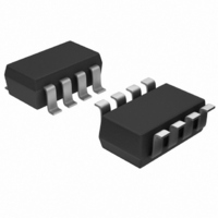
IC ADC 12BIT DFF 600KSPS SOT23-8
Manufacturer
Analog Devices Inc
Datasheet
1.AD7453BRTZ-R2.pdf
(20 pages)
Specifications of AD7453ART-REEL7
Design Resources
Measuring -48 V High-Side Current Using AD629, AD8603, AD780, and AD7453 (CN0100)
Number Of Bits
12
Sampling Rate (per Second)
555k
Data Interface
DSP, MICROWIRE™, QSPI™, Serial, SPI™
Number Of Converters
1
Power Dissipation (max)
7.25mW
Voltage Supply Source
Single Supply
Operating Temperature
-40°C ~ 85°C
Mounting Type
Surface Mount
Package / Case
SOT-23-8
Lead Free Status / RoHS Status
Contains lead / RoHS non-compliant


PIN CONFIGURATION AND FUNCTION DESCRIPTIONS
Table 4. Pin Function Descriptions
Mnemonic
V
V
V
GND
CS
SDATA
SCLK
V
REF
IN+
IN–
DD
Function
Reference Input for the AD7453. An external reference in the range 100 mV to V
reference input is 2.5 V. This pin should be decoupled to GND with a capacitor of at least 0.1 µF.
Noninverting Analog Input.
Inverting Input. This pin sets the ground reference point for the V
pseudo ground.
Analog Ground. Ground reference point for all circuitry on the AD7453. All analog input signals and any external reference
signal should be referred to this GND voltage.
Chip Select. Active low logic input. This input provides the dual function of initiating a conversion on the AD7453 and
framing the serial data transfer.
Serial Data. Logic output. The conversion result from the AD7453 is provided on this output as a serial data stream. The bits
are clocked out on the falling edge of the SCLK input. The data stream of the AD7453 consists of four leading zeros followed
by the 12 bits of conversion data that are provided MSB first. The output coding is straight (natural) binary.
Serial Clock. Logic input. SCLK provides the serial clock for accessing data from the part. This clock input is also used as the
clock source for the conversion process.
Power Supply Input. V
tantalum capacitor.
DD
is 2.7 V to 5.25 V. This supply should be decoupled to GND with a 0.1 µF capacitor and a 10 µF
SDATA
Figure 4. Pin Function Descriptions
SCLK
V
CS
DD
Rev. B | Page 7 of 20
1
2
3
4
(Not to Scale)
AD7453
TOP VIEW
8
7
6
5
V
V
V
GND
IN+
REF
IN+
IN–
input. Connect to ground or to a dc offset to provide a
DD
must be applied to this input. The specified
AD7453
Related parts for AD7453ART-REEL7
Image
Part Number
Description
Manufacturer
Datasheet
Request
R

Part Number:
Description:
Pseudo Differential, 555 kSPS, 12-Bit A/D Converter in 8-Lead SOT-23
Manufacturer:
Analog Devices
Datasheet:

Part Number:
Description:
±1.7g Dual-Axis IMEMS Accelerometer Evaluation Board
Manufacturer:
Analog Devices Inc
Datasheet:

Part Number:
Description:
Inertial Sensor Evaluation System
Manufacturer:
Analog Devices Inc
Datasheet:
Part Number:
Description:
Manufacturer:
Analog Devices Inc
Datasheet:
Part Number:
Description:
Manufacturer:
Analog Devices Inc
Datasheet:
Part Number:
Description:
Manufacturer:
Analog Devices Inc
Datasheet:
Part Number:
Description:
Manufacturer:
Analog Devices Inc
Datasheet:
Part Number:
Description:
Manufacturer:
Analog Devices Inc
Datasheet:
Part Number:
Description:
Manufacturer:
Analog Devices Inc
Datasheet:
Part Number:
Description:
Manufacturer:
Analog Devices Inc
Datasheet:
Part Number:
Description:
Manufacturer:
Analog Devices Inc
Datasheet:
Part Number:
Description:
Manufacturer:
Analog Devices Inc
Datasheet:
Part Number:
Description:
Manufacturer:
Analog Devices Inc
Datasheet: