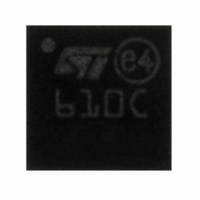
STMPE610QTR STMicroelectronics, STMPE610QTR Datasheet - Page 13

STMPE610QTR
Manufacturer Part Number
STMPE610QTR
Description
IC CTLR ADV TOUCH SCREEN 16-QFN
Manufacturer
STMicroelectronics
Series
S-Touch™r
Type
Resistiver
Specifications of STMPE610QTR
Touch Panel Interface
4-Wire
Number Of Inputs/keys
1 TSC
Resolution (bits)
12 b
Data Interface
I²C, Serial, SPI™
Data Rate/sampling Rate (sps, Bps)
180k
Voltage Reference
External
Voltage - Supply
1.65 V ~ 3.6 V
Operating Temperature
-40°C ~ 85°C
Mounting Type
Surface Mount
Package / Case
16-QFN
Voltage Supply Source
Single Supply
Sampling Rate (per Second)
180k
Resolution
12 bit
Number Of Adc Inputs
6
Interface Type
I2C, SPI
Supply Voltage (max)
3.6 V
Supply Voltage (min)
1.65 V
Maximum Operating Temperature
+ 85 C
Minimum Operating Temperature
- 40 C
Mounting Style
SMD/SMT
Lead Free Status / RoHS Status
Lead free / RoHS Compliant
Other names
497-8825-2
Available stocks
Company
Part Number
Manufacturer
Quantity
Price
STMPE610
5.1.2
5.1.3
5.2
Register write
The following steps need to be followed for register write through SPI.
1.
2.
3.
4.
5.
Termination of data transfer
A transfer can be terminated before the last launch edge by deasserting the CS_n signal. If
the last launch clock is detected, it is assumed that the data transfer is successful.
SPI timing modes
The SPI timing modes are defined by CPHA and CPOL,CPHA and CPOL are read from the
"SDAT" and "A0" pins during power-up reset. The following four modes are defined
according to this setting.
Table 9.
The clocking diagrams of these modes are shown in ON reset. The device always operates
in mode 0. Once the bits are set in the SPICON register, the mode change takes effect on
the next transaction defined by the CS_n pin being deasserted and asserted.
CPOL_N (SDAT pin)
Assert CS_n by driving a '0' on this pin.
Drive a '0' on the first SCL launch clock on MOSI to select a write operation.
The next 7 bits on MOSI denote the 7-bit register address (MSB first).
The next byte on the MOSI denotes data to be written.
The following transmissions on MOSI are considered byte-sized data. The register
address to which the following data is written depends on whether the autoincrement
bit in the SPICON register is set. If this bit has been set previously, the register address
is incremented for data writes.
1
1
0
0
SPI timing modes
Doc ID 15432 Rev 3
CPOL
0
0
1
1
CPHA (ADDR pin)
0
1
0
1
Mode
SPI interface
0
1
2
3
13/56


