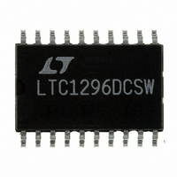
LTC1296DCSW Linear Technology, LTC1296DCSW Datasheet - Page 24

LTC1296DCSW
Manufacturer Part Number
LTC1296DCSW
Description
IC DATA ACQ SYSTEM 12BIT 20-SOIC
Manufacturer
Linear Technology
Type
Data Acquisition System (DAS), ADCr
Datasheet
1.LTC1296CCSWPBF.pdf
(28 pages)
Specifications of LTC1296DCSW
Resolution (bits)
12 b
Sampling Rate (per Second)
46.5k
Data Interface
Serial, Parallel
Voltage Supply Source
Dual ±
Voltage - Supply
±5V
Operating Temperature
0°C ~ 70°C
Mounting Type
Surface Mount
Package / Case
20-SOIC (7.5mm Width)
Lead Free Status / RoHS Status
Contains lead / RoHS non-compliant
Other names
LTC1296DCS
Available stocks
Company
Part Number
Manufacturer
Quantity
Price
Part Number:
LTC1296DCSW
Manufacturer:
LINEAR/凌特
Quantity:
20 000
Company:
Part Number:
LTC1296DCSW#PBF
Manufacturer:
LT
Quantity:
2 122
LTC1293/LTC1294/LTC1296
A
24
This means four channels can handle 7mA of input current
each. Reducing CLK frequency from a maximum of 1MHz
(See typical performance characteristics curves Maxi-
mum CLK Frequency vs Source Resistance and Sample
and Hold Acquisition Time vs Source Resistance) allows
the use of larger current limiting resistors. The “+” input
can accept a resistor value of 1kΩ but the “–” input cannot
accept more than 250Ω when the maximum clock fre-
quency of 1MHz is used. If the LTC1293/4/6 is clocked at
the maximum clock frequency and 250Ω is not enough to
current limit the “–” input source then the clamp diodes
are recommended (Figures 20a and 20b). The reason for
the limit on the resistor value is the MSB bit test is affected
by the value of the resistor placed at the “–” input (see
discussion on Analog Inputs and the typical performance
characteristics curve Maximum CLK Frequency vs Source
Resistance).
If V
turned on first, then V
connecting a diode from V
Figure 21).
For dual supplies (bipolar mode) placing two Schottky
diodes from V
PPLICATI
CC
and V
Figure 20a. Overvoltage Protection for Inputs
Figure 19. Overvoltage Protection for Inputs
1N4148 DIODES
REF
CC
250Ω
1k
are not tied together, then V
O
and V
U
REF
S
–
+
–
DGND
DGND
to ground (Figure 22) will prevent
LTC1293/4/6
LTC1293/4/6
. If this sequence cannot be met
REF
I FOR ATIO
U
to V
AGND
AGND
V
V
V
CC
V
CC
–
CC
–
LTC1293 F19
is recommended (see
W
LTC1293 F20a
+5V
–5V
–5V
+5V
CC
should be
U
power supply reversal from occuring when an input source
is applied to the analog MUX before power is applied to the
device. Power supply reversal occurs, for example, if the
input is pulled below V
below ground which could cause the device not to power
up properly. Likewise, if the input is pulled above V
will be pulled a diode drop above ground. If no inputs are
present on the MUX, the Schottky diodes are not required
if V
Because a unique input protection structure is used on the
digital input pins, the signal levels on these pins can
exceed the device V
–
is applied first then V
Figure 20b. Overvoltage Protection for Inputs
Figure 22. Power Supply Reversal
1k
1N4148 DIODES
DGND
DGND
LTC1293/4/6
CC
LTC1293/4/6
without damaging the device.
–
. V
Figure 21
AGND
+
–
DGND
LTC1293/4/6
AGND
V
REF
CC
V
CC
V
CC
–
CC
+
.
will then pull a diode drop
AGND
V
V
CC
–
LTC1293 F21
1N4148
1N5817
1N5817
LTC1293 F22
+5V
LTC1293 F20b
+5V
+5V
–5V
+5V
–5V
CC
129346fs
, V
–


