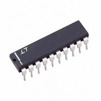
LTC1094ACN Linear Technology, LTC1094ACN Datasheet - Page 8

LTC1094ACN
Manufacturer Part Number
LTC1094ACN
Description
IC DATA ACQ SYS 10BIT 8CH 20-DIP
Manufacturer
Linear Technology
Type
Data Acquisition System (DAS), ADCr
Datasheet
1.LTC1091CN8PBF.pdf
(32 pages)
Specifications of LTC1094ACN
Resolution (bits)
10 b
Data Interface
Serial
Voltage Supply Source
Dual ±
Voltage - Supply
4.5 V ~ 10 V
Operating Temperature
-40°C ~ 85°C
Mounting Type
Through Hole
Package / Case
20-DIP (0.300", 7.62mm)
Lead Free Status / RoHS Status
Contains lead / RoHS non-compliant
Sampling Rate (per Second)
-
Available stocks
Company
Part Number
Manufacturer
Quantity
Price
Company:
Part Number:
LTC1094ACN
Manufacturer:
TI
Quantity:
7 818
Part Number:
LTC1094ACN
Manufacturer:
LT/凌特
Quantity:
20 000
PI FU CTIO S
LTC1091/LTC1092
CS (Pin 1): Chip Select Input. A logic low on this input
enables the LTC1091/LTC1092.
CH0, CH1/+ IN, – IN (Pins 2, 3): Analog Inputs. These
inputs must be free of noise with respect to GND.
GND (Pin 4): Analog Ground. GND should be tied directly
to an analog ground plane.
D
address is shifted into this input.
V
input defines the span of the A/D converter and must be
kept free of noise with respect to AGND.
D
result is shifted out of this output.
CLK (Pin 7): Shift Clock. This clock synchronizes the serial
data transfer.
V
ence Voltage. This pin provides power and defines the
span of the A/D converter. It must be kept free of noise and
ripple by bypassing directly to the analog ground plane.
TYPICAL PERFOR
8
LTC1091/LTC1092
LTC1093/LTC1094
REF
CC
IN
OUT
U
(V
(Pin 5)(LTC1091): Digital Data Input. The multiplexer
(Pin 5)(LTC1092): Reference Input. The reference
(Pin 6): Digital Data Output. The A/D conversion
REF
)(Pin 8)(LTC1091): Positive Supply and Refer-
U
0.6
0.5
0.4
0.3
0.2
0.1
0
–50
LTC1092/LTC1093/LTC1094
Reference Current vs Temperature
–25
U
AMBIENT TEMPERATURE ( C)
0
W
25
A
50
U
CE
75
V
REF
1091/2/3/4 G28
100
C
= 5V
HARA TERISTICS
125
C
V
provides power to the A/D converter. It must be kept free
of noise and ripple by bypassing directly to the analog
ground plane.
LTC1093/LTC1094
CH0 to CH5/CH0 to CH7 (Pins 1 to 6/Pins 1 to 8): Analog
Inputs. The analog inputs must be free of noise with
respect to AGND.
COM (Pin 7/Pin 9): Common. The common pin defines the
zero reference point for all single-ended inputs. It must be
free of noise and is usually tied to the analog ground plane.
DGND (Pin 8/Pin 10): Digital Ground. This is the ground
for the internal logic. Tie to the ground plane.
V
negative potential in the circuit. (Ground in single supply
applications.)
AGND (Pin 10/Pin 12): Analog Ground. AGND should be
tied directly to the analog ground plane.
CC
–
(Pin 9/Pin 11): Negative Supply. Tie V
(Pin 8 )(LTC1092): Positive Supply Voltage. This pin
1000
600
900
800
700
500
400
300
200
100
0
–50
LTC1093/LTC1094 Input Channel
Leakage Current vs Temperature
–25
AMBIENT TEMPERATURE ( C)
0
25
50
OFF-CHANNEL
ON-CHANNEL
GUARANTEED
75
1091/2/3/4 G29
100
125
–
to most


