AD7891APZ-1 Analog Devices Inc, AD7891APZ-1 Datasheet - Page 6
AD7891APZ-1
Manufacturer Part Number
AD7891APZ-1
Description
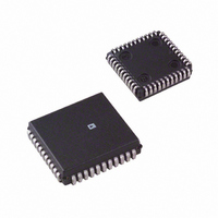
IC DAS 12BIT 8CH 44-PLCC
Manufacturer
Analog Devices Inc
Type
Data Acquisition System (DAS)r
Datasheet
1.AD7891BSZ-2.pdf
(20 pages)
Specifications of AD7891APZ-1
Resolution (bits)
12 b
Data Interface
Serial, Parallel
Sampling Rate (per Second)
500k
Voltage Supply Source
Single Supply
Voltage - Supply
5V
Operating Temperature
-40°C ~ 85°C
Mounting Type
Surface Mount
Package / Case
44-PLCC
Sampling Rate
500kSPS
Input Channel Type
Single Ended
Supply Voltage Range - Analog
4.75V To 5.25V
Supply Current
20mA
Lead Free Status / RoHS Status
Lead free / RoHS Compliant
Available stocks
Company
Part Number
Manufacturer
Quantity
Price
Company:

Part Number:
AD7891APZ-1
Manufacturer:
Analog Devices Inc
Quantity:
10 000
Part Number:
AD7891APZ-1
Manufacturer:
ADI/亚德诺
Quantity:
20 000
Company:
Part Number:
AD7891APZ-1REEL
Manufacturer:
Analog Devices Inc
Quantity:
10 000


AD7891
PLCC
Pin No. Pin No. Mnemonic
1–5
34–44
10, 19
11, 33
20
6
9
7
30
32
12
MQFP
28–43
4, 13
5, 27
14
44
3
1
24
26
6
V
V
AGND
DGND
STANDBY
REF OUT/REF IN
REF GND
CONVST
EOC
MODE
INXA
DD
, V
INXB
Description
Analog Input Channels. The AD7891 contains eight pairs of analog input channels. Each
channel contains two input pins to allow a number of different input ranges to be used
with the AD7891. There are two possible input voltage ranges on the AD7891-1. The
± 5 V input range is selected by connecting the input voltage to both V
while the ± 10 V input range is selected by applying the input voltage to V
necting V
2.5 V input range is selected by connecting the analog input voltage to both V
0 V to 5 V input range is selected by applying the input voltage to V
V
voltage to V
from a low impedance source). The channel to be converted is selected by the A2, A1,
and A0 bits of the control register. In the parallel interface mode, these bits are available as
three data input lines (DB3 to DB5) in a parallel write operation. While in the serial inter-
face mode, these three bits are accessed via the DATA IN line in a serial write operation.
The multiplexer has guaranteed break-before-make operation.
Positive Supply Voltage, 5 V ± 5%.
Analog Ground. Ground reference for track/hold, comparator, and DAC.
Digital Ground. Ground reference for digital circuitry.
Standby Mode Input. TTL compatible input used to put the device into the power
save or standby mode. The STANDBY input is high for normal operation and low for
standby operation.
Voltage Reference Output/Input. The part can either be used with its own internal refer-
ence or with an external reference source. The on-chip 2.5 V reference voltage is pro-
vided at this pin. When using this internal reference as the reference source for the
part, REF OUT should be decoupled to REF GND with a 0.1 mF disc ceramic capaci-
tor. The output impedance of the reference source is typically 2 kW. When using an
external reference source as the reference voltage for the part, the reference source
should be connected to this pin. This overdrives the internal reference and provides the
reference source for the part. The reference pin is buffered on-chip but must be able to
sink or source current through this 2 kW resistor to the output of the on-chip reference.
The nominal reference voltage for correct operation of the AD7891 is 2.5 V.
Reference Ground. Ground reference for the part’s on-chip reference buffer. The REF
OUT pin of the part should be decoupled with a 0.1 mF capacitor to this REF GND
pin. If the AD7891 is used with an external reference, the external reference should also
be decoupled to this pin. The REF GND pin should be connected to the AGND pin
or the system’s AGND plane.
Convert Start. Edge-triggered logic input. A low-to-high transition on this input puts
the track/hold into hold and initiates conversion. When changing channels on the part,
sufficient time should be given for multiplexer settling and track/hold acquisition between
the channel change and the rising edge of CONVST.
End-of-Conversion. Active low logic output indicating converter status. The end of con-
version is signified by a low-going pulse on this line. The duration of this EOC pulse is
nominally 80 ns.
Interface Mode. Control input that determines the interface mode for the part. With this
pin at a logic low, the AD7891 is in its serial interface mode; with this pin at a logic high,
the device is in its parallel interface mode.
INXB
PIN FUNCTION DESCRIPTIONS
to AGND while the ± 2.5 V input range is selected by connecting the analog input
INXB
INXA
to AGND. The AD7891-2 has three possible input ranges. The 0 V to
and connecting V
–6–
INXB
to REF IN (provided this REF IN voltage comes
INXA
INXA
INXA
and connecting
INXA
and V
and V
and con-
INXB
INXB
REV. D
,
; the
Related parts for AD7891APZ-1
Image
Part Number
Description
Manufacturer
Datasheet
Request
R

Part Number:
Description:
RF/COAXIAL ADAPTER, TRB JACK-TRB JACK
Manufacturer:
TROMPETER ELECTRONICS
Datasheet:

Part Number:
Description:
±1.7g Dual-Axis IMEMS Accelerometer Evaluation Board
Manufacturer:
Analog Devices Inc
Datasheet:

Part Number:
Description:
Inertial Sensor Evaluation System
Manufacturer:
Analog Devices Inc
Datasheet:
Part Number:
Description:
Manufacturer:
Analog Devices Inc
Datasheet:
Part Number:
Description:
Manufacturer:
Analog Devices Inc
Datasheet:
Part Number:
Description:
Manufacturer:
Analog Devices Inc
Datasheet:
Part Number:
Description:
Manufacturer:
Analog Devices Inc
Datasheet:
Part Number:
Description:
Manufacturer:
Analog Devices Inc
Datasheet:
Part Number:
Description:
Manufacturer:
Analog Devices Inc
Datasheet:
Part Number:
Description:
Manufacturer:
Analog Devices Inc
Datasheet:
Part Number:
Description:
Manufacturer:
Analog Devices Inc
Datasheet:
Part Number:
Description:
Manufacturer:
Analog Devices Inc
Datasheet:
Part Number:
Description:
Manufacturer:
Analog Devices Inc
Datasheet: