AD7891APZ-1 Analog Devices Inc, AD7891APZ-1 Datasheet - Page 9
AD7891APZ-1
Manufacturer Part Number
AD7891APZ-1
Description
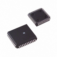
IC DAS 12BIT 8CH 44-PLCC
Manufacturer
Analog Devices Inc
Type
Data Acquisition System (DAS)r
Datasheet
1.AD7891BSZ-2.pdf
(20 pages)
Specifications of AD7891APZ-1
Resolution (bits)
12 b
Data Interface
Serial, Parallel
Sampling Rate (per Second)
500k
Voltage Supply Source
Single Supply
Voltage - Supply
5V
Operating Temperature
-40°C ~ 85°C
Mounting Type
Surface Mount
Package / Case
44-PLCC
Sampling Rate
500kSPS
Input Channel Type
Single Ended
Supply Voltage Range - Analog
4.75V To 5.25V
Supply Current
20mA
Lead Free Status / RoHS Status
Lead free / RoHS Compliant
Available stocks
Company
Part Number
Manufacturer
Quantity
Price
Company:

Part Number:
AD7891APZ-1
Manufacturer:
Analog Devices Inc
Quantity:
10 000
Part Number:
AD7891APZ-1
Manufacturer:
ADI/亚德诺
Quantity:
20 000
Company:
Part Number:
AD7891APZ-1REEL
Manufacturer:
Analog Devices Inc
Quantity:
10 000


TERMINOLOGY
Signal-to-(Noise + Distortion) Ratio
This is the measured ratio of signal to (noise + distortion) at the
output of the ADC. The signal is the rms amplitude of the
fundamental. Noise is the rms sum of all nonfundamental
signals up to half the sampling frequency (f
The ratio is dependent upon the number of quantization levels
in the digitization process; the more levels, the smaller the quan-
tization noise. The theoretical signal-to-(noise +distortion) ratio
for an ideal N-bit converter with a sine wave input is given by
Therefore, for a 12-bit converter, this is 74 dB.
Total Harmonic Distortion (THD)
THD is the ratio of the rms sum of harmonics to the
fundamental. For the AD7891, it is defined as
where V
V
sixth harmonics.
Peak Harmonic or Spurious Noise
Peak harmonic or spurious noise is defined as the ratio of the rms
value of the next largest component in the ADC output spectrum
(up to f
Normally, the value of this specification is determined by the larg-
est harmonic in the spectrum, but for parts where the harmonics
are buried in the noise floor, it is a noise peak.
Intermodulation Distortion
With inputs consisting of sine waves at two frequencies, fa and
fb, any active device with nonlinearities creates distortion
products at sum and difference frequencies of mfa ± nfb, where
m, n = 0, 1, 2, 3, and so on. Intermodulation terms are those for
which neither m nor n are equal to zero. For example, the
second-order terms include (fa + fb) and (fa – fb), while the
third-order terms include (2fa + fb), (2fa – fb), (fa + 2fb), and
(fa – 2fb).
The AD7891 is tested using the CCIF standard where two
input frequencies near the top end of the input bandwidth are
used. In this case, the second- and third-order terms are of
different significance. The second-order terms are usually dis-
tanced in frequency from the original sine waves while the third-
order terms are usually at a frequency close to the input
frequencies. As a result, the second- and-third order terms are
specified separately. The calculation of the intermodulation
distortion is as per the THD specification where it is the ratio of
the rms sum of the individual distortion products to the rms
amplitude of the fundamental expressed in dBs.
REV. D
4
, V
5
and V
Signal-to-(Noise + Distortion) = (6.02N + 1.76) dB
S
THD dB
/2 and excluding dc) to the rms value of the fundamental.
1
is the rms amplitude of the fundamental and V
6
( )
are the rms amplitudes of the second through the
=
20
log
V
2
2
+
V
3
2
+
V
V
1
4
2
S
+
/2), excluding dc.
V
5
2
+
V
6
2
2
, V
3
,
–9–
Channel-to-Channel Isolation
Channel-to-channel isolation is a measure of the level of
crosstalk between channels. It is measured by applying a full-
scale 20 kHz (AD7891-1) or 100 kHz (AD7891-2) sine wave
signal to one input channel and determining how much that
signal is attenuated in each of the other channels. The figure
given is the worst case across all eight channels.
Relative Accuracy
Relative accuracy or endpoint nonlinearity is the maximum
deviation from a straight line passing through the endpoints of
the ADC transfer function.
Differential Nonlinearity
This is the difference between the measured and the ideal 1 LSB
change between any two adjacent codes in the ADC.
Positive Full-Scale Error (AD7891-1,
AD7891-2,
This is the deviation of the last code transition (01. . .110 to
01. . .111) from the ideal 4 ¥ REF IN – 3/2 LSB (AD7891-1
± 10 V range), 2 ¥ REF IN – 3/2 LSB (AD7891-1 ± 5 V range),
or REF IN – 3/2 LSB (AD7891-2, ± 2.5 V range), after the
bipolar zero error has been adjusted out.
Positive Full-Scale Error (AD7891-2, 0 V to 5 V and 0 V to 2.5 V)
This is the deviation of the last code transition (11. . .110 to
11. . .111) from the ideal 2 ¥ REF IN – 3/2 LSB (0 V to 5 V
range), or REF IN – 3/2 LSB (0 V to 2.5 V range), after the
unipolar offset error has been adjusted out.
Bipolar Zero Error (AD7891-1, 10 V and 5 V; AD7891-2, 2.5 V)
This is the deviation of the midscale transition (all 0s to all 1s)
from the ideal AGND – 1/2 LSB.
Unipolar Offset Error (AD7891-2, 0 V to 5 V and 0 V to 2.5 V)
This is the deviation of the first code transition (00. . .000 to
00. . .001) from the ideal AGND + 1/2 LSB.
Negative Full-Scale Error (AD7891-1,
AD7891-2,
This is the deviation of the first code transition (10. . .000 to
10. . .001) from the ideal –4 ¥ REF IN + 1/2 LSB (AD7891-1
±10 V range), –2 ¥ REF IN + 1/2 LSB (AD7891-1 ± 5 V range),
or –REF IN + 1/2 LSB (AD7891-2, ± 2.5 V range), after bipolar
zero error has been adjusted out.
Track/Hold Acquisition Time
Track/hold acquisition time is the time required for the output of
the track/hold amplifier to reach its final value, within ± 1/2 LSB,
after the end of conversion (the point at which the track/hold
returns to track mode). It also applies to situations where a
change in the selected input channel takes place or where there
is a step input change on the input voltage applied to the selected
V
duration of the track/hold acquisition time after the end of
conversion or after a channel change/step input change to V
before starting another conversion, to ensure the part operates
to specification.
IN
input of the AD7891. It means the user must wait for the
2.5 V)
2.5 V)
10 V and
10 V and
AD7891
5 V;
5 V;
IN
Related parts for AD7891APZ-1
Image
Part Number
Description
Manufacturer
Datasheet
Request
R

Part Number:
Description:
RF/COAXIAL ADAPTER, TRB JACK-TRB JACK
Manufacturer:
TROMPETER ELECTRONICS
Datasheet:

Part Number:
Description:
±1.7g Dual-Axis IMEMS Accelerometer Evaluation Board
Manufacturer:
Analog Devices Inc
Datasheet:

Part Number:
Description:
Inertial Sensor Evaluation System
Manufacturer:
Analog Devices Inc
Datasheet:
Part Number:
Description:
Manufacturer:
Analog Devices Inc
Datasheet:
Part Number:
Description:
Manufacturer:
Analog Devices Inc
Datasheet:
Part Number:
Description:
Manufacturer:
Analog Devices Inc
Datasheet:
Part Number:
Description:
Manufacturer:
Analog Devices Inc
Datasheet:
Part Number:
Description:
Manufacturer:
Analog Devices Inc
Datasheet:
Part Number:
Description:
Manufacturer:
Analog Devices Inc
Datasheet:
Part Number:
Description:
Manufacturer:
Analog Devices Inc
Datasheet:
Part Number:
Description:
Manufacturer:
Analog Devices Inc
Datasheet:
Part Number:
Description:
Manufacturer:
Analog Devices Inc
Datasheet:
Part Number:
Description:
Manufacturer:
Analog Devices Inc
Datasheet: