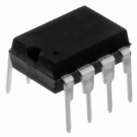
MCP4151-104E/P Microchip Technology, MCP4151-104E/P Datasheet - Page 31

MCP4151-104E/P
Manufacturer Part Number
MCP4151-104E/P
Description
IC POT DGTL SNGL 100K SPI 8DIP
Manufacturer
Microchip Technology
Specifications of MCP4151-104E/P
Package / Case
8-DIP (0.300", 7.62mm)
Taps
257
Resistance (ohms)
100K
Number Of Circuits
1
Temperature Coefficient
150 ppm/°C Typical
Memory Type
Volatile
Interface
SPI Serial
Voltage - Supply
1.8 V ~ 5.5 V
Operating Temperature
-40°C ~ 125°C
Mounting Type
Through Hole
Resistance In Ohms
100K
Number Of Pots
Single
Taps Per Pot
256
Resistance
100 KOhms
Wiper Memory
Volatile
Digital Interface
Serial (SPI)
Operating Supply Voltage
2.5 V or 3.3 V or 5 V
Supply Current
1 mA
Maximum Operating Temperature
+ 125 C
Minimum Operating Temperature
- 40 C
Mounting Style
Through Hole
Supply Voltage (max)
5.5 V
Supply Voltage (min)
1.8 V
Lead Free Status / RoHS Status
Lead free / RoHS Compliant
Lead Free Status / RoHS Status
Lead free / RoHS Compliant, Lead free / RoHS Compliant
Available stocks
Company
Part Number
Manufacturer
Quantity
Price
Company:
Part Number:
MCP4151-104E/P
Manufacturer:
NXP
Quantity:
1 799
3.0
The descriptions of the pins are listed in
Additional descriptions of the device pins follows.
TABLE 3-1:
© 2007 Microchip Technology Inc.
Legend:
Note 1:
Rheo Pot
8L
—
—
—
—
—
—
—
(4)
1
2
3
4
5
6
7
8
Single
2:
3:
4:
PIN DESCRIPTIONS
8L
—
—
—
—
—
—
—
(4)
1
2
3
4
5
6
7
8
The 8-lead Single Potentiometer devices are pin limited so the SDO pin is multiplexed with the SDI pin
(SDI/SDO pin). After the Address/Command (first 6-bits) are received, If a valid Read command has been
requested, the SDO pin starts driving the requested read data onto the SDI/SDO pin.
The pin’s “smart” pull-up shuts off while the pin is forced low. This is done to reduce the standby and shut-
down current.
The SDO is an open drain output, which uses the internal “smart” pull-up. The SDI input data rate can be
at the maximum SPI frequency. the SDO output data rate will be limited by the “speed” of the pull-up, cus-
tomers can increase the rate with external pull-up resistors.
The DFN and QFN packages have a contact on the bottom of the package. This contact is conductively
connected to the die substrate, and therefore should be unconnected or connected to the same ground as
the device’s V
(1)
HV w/ST = High Voltage tolerant input (with Schmidtt trigger input)
A = Analog pins (Potentiometer terminals)
O = digital output
P = Power
Rheo
10L
PINOUT DESCRIPTION FOR THE MCP413X/415X/423X/425X
10
—
—
—
—
—
(4)
1
2
3
4
5
6
7
8
9
Dual
14L
SS
10
12
13
14
11
—
—
1
2
3
4
5
6
7
8
9
pin.
Pot
11,12 NC
16L
3, 4
16
—
10
13
14
15
(4)
1
2
5
6
7
8
9
Pin
CS
SCK
SDI
SDI/SDO
V
P1B
P1W
P1A
P0A
P0W
P0B
SHDN
SDO
V
Exposed Pad
SS
DD
Symbol
Table
MCP413X/415X/423X/425X
(1, 3)
3-1.
I/O
I/O
—
—
—
—
O
A
A
A
A
A
A
I
I
I
I
HV w/ST
HV w/ST
HV w/ST
HV w/ST
HV w/ST
Analog
Analog
Analog
Analog
Analog
Analog
Buffer
Type
—
—
O
P
P
I = digital input (high Z)
I/O = Input / Output
down
Pull-up/
“smart”
“smart”
“smart”
“smart”
“smart”
Weak
No
No
No
No
No
No
No
—
—
—
—
(2)
Hardware Shutdown
SPI Chip Select Input
SPI Clock Input
SPI Serial Data Input
SPI Serial Data Input/Output
Ground
Potentiometer 1 Terminal B
Potentiometer 1 Wiper Terminal
Potentiometer 1 Terminal A
Potentiometer 0 Terminal A
Potentiometer 0 Wiper Terminal
Potentiometer 0 Terminal B
SPI Serial Data Out
Positive Power Supply Input
No Connection
Note 4
Standard Function
DS22060A-page 31


