AD5175BRMZ-10 Analog Devices Inc, AD5175BRMZ-10 Datasheet - Page 6
AD5175BRMZ-10
Manufacturer Part Number
AD5175BRMZ-10
Description
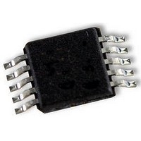
IC DGTL POT 1024POS 10K 10MSOP
Manufacturer
Analog Devices Inc
Datasheet
1.AD5175BRMZ-10-RL7.pdf
(20 pages)
Specifications of AD5175BRMZ-10
Taps
1024
Resistance (ohms)
10K
Number Of Circuits
1
Temperature Coefficient
35 ppm/°C Typical
Memory Type
Non-Volatile
Interface
I²C, 2-Wire Serial
Voltage - Supply
2.7 V ~ 5.5 V, ±2.5 V ~ 2.75 V
Operating Temperature
-40°C ~ 125°C
Mounting Type
Surface Mount
Package / Case
10-MSOP, Micro10™, 10-uMAX, 10-uSOP
Resistance In Ohms
10K
End To End Resistance
10kohm
Resistance Tolerance
-15% To +15%
No. Of Steps
1024
Supply Voltage Range
2.7V To 5.5V, ± 2.7V
Control Interface
I2C, Serial
No. Of Pots
Single
Memory
RoHS Compliant
Rohs Compliant
Yes
Lead Free Status / RoHS Status
Lead free / RoHS Compliant
Available stocks
Company
Part Number
Manufacturer
Quantity
Price
Company:

Part Number:
AD5175BRMZ-10
Manufacturer:
VISHAY
Quantity:
5 015
Part Number:
AD5175BRMZ-10
Manufacturer:
ADI/亚德诺
Quantity:
20 000
Part Number:
AD5175BRMZ-10-RL7
Manufacturer:
ADI/亚德诺
Quantity:
20 000


AD5175
ABSOLUTE MAXIMUM RATINGS
T
Table 3.
Parameter
V
V
V
V
Digital Input and Output Voltage to GND
EXT_CAP to V
I
Operating Temperature Range
Maximum Junction Temperature
Storage Temperature Range
Reflow Soldering
Package Power Dissipation
1
2
3
A
Maximum terminal current is bounded by the maximum current handling of
the switches, maximum power dissipation of the package, and maximum
applied voltage across any two of the A and W terminals at a given
resistance.
Pulse duty factor.
Includes programming of 50-TP memory.
DD
SS
DD
A
A
, I
, V
Pulsed
Continuous
(T
Peak Temperature
Time at Peak Temperature
= 25°C, unless otherwise noted.
W
to GND
to GND
to V
J
W
Frequency > 10 kHz
Frequency ≤ 10 kHz
Maximum)
to GND
SS
1
SS
3
Rating
–0.3 V to +7.0 V
+0.3 V to −7.0 V
7 V
V
−0.3 V to V
7 V
±6 mA/d
±6 mA/√d
±6 mA
−40°C to +125°C
150°C
−65°C to +150°C
260°C
20 sec to 40 sec
(T
SS
J
max − T
− 0.3 V, V
2
2
DD
A
DD
)/θ
+ 0.3 V
+ 0.3 V
JA
Rev. A | Page 6 of 20
Stresses above those listed under Absolute Maximum Ratings
may cause permanent damage to the device. This is a stress
rating only and functional operation of the device at these or
any other conditions above those indicated in the operational
section of this specification is not implied. Exposure to absolute
maximum rating conditions for extended periods may affect
device reliability.
THERMAL RESISTANCE
θ
dependent on the test board and test environment.
Table 4. Thermal Resistance
Package Type
10-Lead LFCSP
10-Lead MSOP
1
ESD CAUTION
JEDEC 2S2P test board, still air (0 m/sec airflow).
JA
is defined by JEDEC specification JESD-51 and the value is
θ
50
135
JA
1
θ
3
N/A
JC
Unit
°C/W
°C/W
Related parts for AD5175BRMZ-10
Image
Part Number
Description
Manufacturer
Datasheet
Request
R

Part Number:
Description:
Low Cost, Laser Trimmed, Precision IC Op Amp
Manufacturer:
AD [Analog Devices]
Datasheet:

Part Number:
Description:
±1.7g Dual-Axis IMEMS Accelerometer Evaluation Board
Manufacturer:
Analog Devices Inc
Datasheet:

Part Number:
Description:
Inertial Sensor Evaluation System
Manufacturer:
Analog Devices Inc
Datasheet:
Part Number:
Description:
Manufacturer:
Analog Devices Inc
Datasheet:
Part Number:
Description:
Manufacturer:
Analog Devices Inc
Datasheet:
Part Number:
Description:
Manufacturer:
Analog Devices Inc
Datasheet:
Part Number:
Description:
Manufacturer:
Analog Devices Inc
Datasheet:
Part Number:
Description:
Manufacturer:
Analog Devices Inc
Datasheet:
Part Number:
Description:
Manufacturer:
Analog Devices Inc
Datasheet:
Part Number:
Description:
Manufacturer:
Analog Devices Inc
Datasheet:
Part Number:
Description:
Manufacturer:
Analog Devices Inc
Datasheet:
Part Number:
Description:
Manufacturer:
Analog Devices Inc
Datasheet:
Part Number:
Description:
Manufacturer:
Analog Devices Inc
Datasheet: