X9271UV14Z-2.7 Intersil, X9271UV14Z-2.7 Datasheet
X9271UV14Z-2.7
Specifications of X9271UV14Z-2.7


Related parts for X9271UV14Z-2.7


X9271UV14Z-2.7 Summary of contents
Page 1
... V SS CAUTION: These devices are sensitive to electrostatic discharge; follow proper IC Handling Procedures. 1-888-INTERSIL or 1-888-352-6832 XDCP is a trademark of Intersil Americas Inc. Copyright Intersil Americas Inc. 2005. All Rights Reserved All other trademarks mentioned are the property of their respective owners. X9271 FN8174.2 (XDCP) ...
Page 2
... X9271TV I X9271TV14IZ* (Note) X9271TV ZI X9271TV14Z* (Note) X9271TV Z X9271UV14-2.7* X9271UV F X9271UV14I-2.7* X9271UV G X9271UV14IZ-2.7* (Note) X9271UV ZF X9271UV14Z-2.7* (Note) X9271UV ZF X9271TV14-2.7* X9271TV F X9271TV14I-2.7* X9271TV G X9271TV14IZ-2.7* (Note) X9271TV ZG X9271TV14Z-2.7* (Note) X9271TV ZF *Add "T1" suffix for tape and reel. NOTE: Intersil Pb-free plus anneal products employ special Pb-free material sets; molding compounds/die attach materials and 100% matte tin plate termination finish, which are RoHS compliant and compatible with both SnPb and Pb-free soldering operations ...
Page 3
DETAILED FUNCTIONAL DIAGRAM V CC HOLD CS SCK INTERFACE SO AND CONTROL SI CIRCUITRY CIRCUIT LEVEL APPLICATIONS • Vary the gain of a voltage amplifier • Provide programmable dc reference voltages for comparators and detectors ...
Page 4
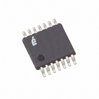
PIN CONFIGURATION TSSOP X9271 SCK PIN ASSIGNMENTS TSSOP Symbol SCK ...
Page 5
... Other Pins ARDWARE RITE ROTECT The WP pin when LOW prevents nonvolatile writes to the Data Registers ONNECT No connect pins should be left floating. This pins are used for Intersil manufacturing and testing purposes AND UPPLY (WP) NPUT FN8174.2 November 22, 2005 ...
Page 6
PRINCIPLES OF OPERATION Device Description S I ERIAL NTERFACE The X9271 supports the SPI interface hardware conventions. The device is accessed via the SI input with data clocked in on the rising SCK. CS must be LOW and the HOLD ...
Page 7
DEVICE DESCRIPTION Wiper Counter Register (WCR) The X9271 contains a Wiper Counter Register for the DCP potentiometer. The Wiper Counter Register can be envisioned as a 8-bit parallel and serial load counter with its outputs decoded to select one of ...
Page 8
DEVICE DESCRIPTION Instructions I B (ID A) DENTIFICATION YTE AND The first byte sent to the X9271 from the host, following a CS going HIGH to LOW, is called the Identification byte. The most significant four bits of the slave ...
Page 9
Table 5. Instruction Byte Format Instruction Opcode (MSB) DEVICE DESCRIPTION Instructions Five of the eight instructions are three bytes in length. These instructions are: – Read Wiper Counter Register – read the current wiper position of the ...
Page 10
Figure 2. Two-Byte Instruction Sequence CS SCK ID3 ID2 ID1 ID0 Device ID Figure 3. Three-Byte Instruction Sequence (Write) CS SCL ID3 ID2 ID1 ID0 ...
Page 11
Figure 5. Increment/Decrement Instruction Sequence CS SCL ID3 ID2 ID1 ID0 0 0 Internal Device ID Address Figure 6. Increment/Decrement Timing Limits SCK INC/DEC CMD ISSUED Table 6. Instruction Set ...
Page 12
INSTRUCTION FORMAT Read Wiper Counter Register (WCR) Device Type Device Identifier Addresses CS Falling Edge Write Wiper Counter Register (WCR) Device Type Device Identifier Addresses CS ...
Page 13
Transfer Data Register (DR) to Wiper Counter Register (WCR) Device Type Device CS Identifier Addresses Falling Edge Increment/Decrement Wiper Counter Register (WCR) Device Type Device CS Identifier Addresses Falling Edge ...
Page 14
ABSOLUTE MAXIMUM RATINGS Temperature under bias..................... -65°C to +135°C Storage temperature ......................... -65°C to +150°C Voltage on SCK any address input with respect to V ................................. -1V to +7V SS ∆ )|..................................................... 5. Lead ...
Page 15
D.C. OPERATING CHARACTERISTICS Symbol Parameter I V supply current CC1 CC (active supply current CC2 CC (nonvolatile write current (standby Input leakage current LI I Output leakage current LO V Input HIGH voltage ...
Page 16
EQUIVALENT A.C. LOAD CIRCUIT 5V 1462Ω SO pin 2714Ω 100pF AC TIMING Symbol f SSI/SPI clock frequency SCK t SSI/SPI clock cycle time CYC t SSI/SPI clock high time WH t SSI/SPI clock low time WL t Lead time LEAD ...
Page 17
HIGH-VOLTAGE WRITE CYCLE TIMING Symbol t High-voltage write cycle time (store instructions) WR XDCP TIMING Symbol t Wiper response time after the third (last) power supply is stable WRPO t Wiper response time after instruction issued (all load instructions) WRL ...
Page 18
TIMING DIAGRAMS Input Timing CS t LEAD SCK MSB SI High Impedance SO Output Timing CS SCK t V MSB SO ADDR SI Hold Timing CS SCK HOLD 18 X9271 t CYC ...
Page 19
XDCP Timing (for All Load Instructions) CS SCK MSB SI VWx High Impedance SO Write Protect and Device Address Pins Timing X9271 ... t WRL ... (Any Instruction WPASU WPAH LSB FN8174.2 November ...
Page 20
APPLICATIONS INFORMATION Basic Configurations of Electronic Potentiometers V R Three terminal Potentiometer; Variable voltage divider Application Circuits Noninverting Amplifier – (1 Offset Voltage Adjustment R 1 ...
Page 21
Application Circuits (continued) Attenuator – -1/2 ≤ G ≤ +1/2 Inverting Amplifier ...
Page 22
... Accordingly, the reader is cautioned to verify that data sheets are current before placing orders. Information furnished by Intersil is believed to be accurate and reliable. However, no responsibility is assumed by Intersil or its subsidiaries for its use; nor for any infringements of patents or other rights of third parties which may result from its use ...