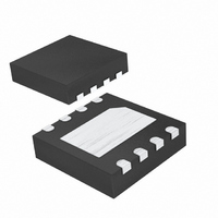
MAX5527GTA+T Maxim Integrated Products, MAX5527GTA+T Datasheet - Page 2

MAX5527GTA+T
Manufacturer Part Number
MAX5527GTA+T
Description
IC POT DGTL 1TIME PROGR 8-TDFN
Manufacturer
Maxim Integrated Products
Datasheet
1.MAX5527GUA.pdf
(12 pages)
Specifications of MAX5527GTA+T
Taps
64
Resistance (ohms)
100K
Number Of Circuits
1
Temperature Coefficient
35 ppm/°C Typical
Memory Type
Non-Volatile
Interface
Up/Down
Voltage - Supply
2.7 V ~ 5.25 V
Operating Temperature
-40°C ~ 105°C
Mounting Type
Surface Mount
Package / Case
8-TDFN Exposed Pad
Resistance In Ohms
100K
Lead Free Status / RoHS Status
Lead free / RoHS Compliant
ABSOLUTE MAXIMUM RATINGS
V
PV to GND ...........................................................-0.3V to +12.0V
All Other Pins to GND.................................-0.3V to (V
Maximum Continuous Current into H, L, and W
One-Time Programmable, Linear-Taper Digital
Potentiometers
ELECTRICAL CHARACTERISTICS
(V
= +25°C.) (Note 1)
Stresses beyond those listed under “Absolute Maximum Ratings” may cause permanent damage to the device. These are stress ratings only, and functional
operation of the device at these or any other conditions beyond those indicated in the operational sections of the specifications is not implied. Exposure to
absolute maximum rating conditions for extended periods may affect device reliability.
2
DC PERFORMANCE
Resolution
End-to-End Resistance
End-to-End Resistance
Temperature Coefficent
Resistance Ratio Temperature
Coefficient
Integral Nonlinearity
Differential Nonlinearity
Full-Scale Error
Zero-Scale Error
Wiper Resistance (Note 2)
DYNAMIC CHARACTERISTICS
Wiper -3dB Bandwidth (Note 3)
Total Harmonic Distortion
DD
MAX5527 ......................................................................±0.5mA
MAX5528 ......................................................................±1.0mA
MAX5529 ......................................................................±2.0mA
DD
_______________________________________________________________________________________
to GND ...........................................................-0.3V to +6.0V
= +2.7V to +5.5V, V
PARAMETER
H
= V
DD
, V
L
SYMBOL
= GND, T
DNL
TC
INL
R
W
R
A
MAX5527
MAX5528
MAX5529
MAX5527/MAX5528
MAX5529
Potentiometer configuration, no load,
Figure 1
Potentiometer configuration, no load,
Figure 1
Potentiometer configuration, no load,
Figure 1
Potentiometer configuration, no load,
Figure 1
V
V
MAX5527
MAX5528
MAX5529
f = 10kHz, midscale, 1V
R
= -40°C to +105°C, unless otherwise noted. Typical values are at V
DD
DD
L
DD
= 100kΩ
≥ 3V
< 3V
+ 0.3V)
CONDITIONS
Continuous Power Dissipation (T
Operating Temperature Range .........................-40°C to +105°C
Junction Temperature ......................................................+150°C
Storage Temperature Range .............................-65°C to +150°C
Lead Temperature (soldering, 10s) .................................+300°C
8-Pin µMAX (derate 4.5mW/°C above +70°C) ..............362mW
8-Pin TDFN (derate 18.2mW/°C above +70°C) .......1454.5mW
RMS
MAX5527
MAX5528
MAX5529
MIN
37.5
7.5
64
75
A
= +70°C)
±0.025
+0.006
-0.005
±0.01
1000
TYP
100
125
100
200
-78
-82
-94
50
10
35
10
90
5
MAX
62.5
12.5
125
200
650
±1
±1
+1
-1
DD
= +5.0V, T
ppm/°C
ppm/°C
UNITS
Taps
LSB
LSB
LSB
LSB
kHz
dB
kΩ
Ω
A


